Introduction
Mg doped GaN grown by MOCVD has high resistivity due to passivation of acceptors by hydrogen incorporated during growth [Reference Pearton, Zolper, Shul and Ren1]. Low resistivity p-type material required for devices can be obtained through post-growth activation by thermal annealing [Reference Nakamura, Mukai, Senoh and Iwasa2, Reference Myers3], low energy electron beam irradiation (LEEBI) [Reference Inamori, Sakai, Tanaka, Amano and Akasaki4, Reference Li and Coleman5] or minority carrier injection [Reference Pearton, Lee and Yuan6, Reference Miyachi, Tanaka, Kimura and Ota7]. Mechanisms for these activation treatments are believed to involve thermal or electronically induced dissociation of hydrogen from acceptors leading to loss of hydrogen from the material, or to a change in atomic configuration or charge state of the hydrogen. In this study we investigate the atomic configuration of hydrogen in GaN. We use density functional theory to predict the lattice configuration for various states of hydrogen in wurtzite Mg doped GaN, and we use ion channeling [Reference Feldman, Mayer and Picraux8] to experimentally examine the hydrogen lattice location.
Experiment
Wurtzite GaN:Mg films with (0001) orientation and thickness in the range of 1.4 −2.3 μm were grown epitaxially by MOCVD on c-oriented sapphire substrates as described elsewhere [Reference Han, Ng, Biefeld, Crawford and Follstaedt9]. The GaN:Mg was doped with Mg at concentrations in the range from 5 to 7×10¹⁹/cm3 as determined by SIMS.
Samples were passivated by exposure to D2 gas at 88 kPa and 700° C for four hours. Conductivity measurements showed this treatment yielded high resistivity passivated films [Reference Myers3]. Other samples were exposed to deuterium ECR plasmas for one hour. The sample temperature during ECR plasma exposure was chosen to be 600°C based on a previous study [Reference Götz, Johnson, Walker, Bour, Amano and Akasaki10] which showed deuterium incorporation into p-type GaN at 600°C but not at 400°C from exposure to remote plasma. During ECR plasma exposure the incident D has about 30 eV of kinetic energy which is high enough to penetrate a few lattice spacings but too low to create bulk defects by atomic collisions [Reference Outten, Barbour and Wampler11].
Prior to gas or plasma exposures the samples were vacuum annealed at 900°C for one hour to remove hydrogen present from growth. After deuterium exposures, the concentration and depth distribution of deuterium in the films was characterized by D(3He,p)α nuclear reaction analysis (NRA) [Reference Myers, Caskey, Rawl and Sisson12] and by secondary ion mass spectroscopy. The D concentrations were uniform throughout the Mg doped region of the films and are given in the legends of figures 1 and 2. In the gas charged sample the D concentration is approximately half the Mg concentration, whereas in the two plasma charged samples the D concentration is higher than the Mg concentration, which indicates that the chemical potential for D from the plasma charging is much higher than from the gas charging.

Figure 1 Effect of channeling on NRA yield for a GaN:Mg sample after exposure to deuterium gas. Filled circles show the initial measurement. Open circles are a repeat measurement at the same position. Inset shows IR absorption peak before ion beam exposure, due to N-D stretch local vibration.

Figure 2 Effect of channeling on NRA yield for two GaN:Mg samples after exposure to deuterium ECR plasma. Inset shows IR absorption peak due to N-D stretch local vibration.
Transmission infrared absorption spectra were also measured in gas and plasma charged samples. In both cases similar absorption peaks were seen at 2320 cm−1 (shown in figures 1 and 2) which were not present prior to deuterium exposure. The increase in energy to 3120 cm−1 seen for this absorption peak in similar samples exposed to hydrogen shows that the absorption peak is due to stretch vibrations of H or D bound to nitrogen. This is also consistent with our observation that the 2320 cm−1 absorption peak disappears when D is removed from the samples by vacuum annealing. The fact that the peak area is similar for the gas and plasma charged samples while the D content is much larger in the plasma charged sample shows that at least in the plasma charged sample much of the D is in an IR inactive state. Similar IR absorption peaks were reported previously for GaN:Mg deuterated with a remote plasma system [Reference Goetz, Johnson, Bour, McCluskey and Haller13] and were ascribed to D at an antibonding position bound to nitrogen neighboring the Mg acceptor.
Ion channeling studies of D were done by counting protons from the D(3He,p)α nuclear reaction using an incident analysis beam of 850 keV 3He+ ions. This gives counts from D to depths of about 1 µm. The analysis beam size was 1×1 mm. Channeling measurements were done with the samples at room temperature. The proton yield was measured as a function of angle between the analyzing ion beam and the crystallographic c-axis of the samples. When the analysis beam is aligned along the c-axis, channeling reduces the ion flux near the rows of host atoms and increases the flux near the center of the open channels, which causes a dip in the NRA yield if the D is near the host atom rows, or conversely, to a peak in yield if the D is near the center of the channel.
Figure 1 shows the measured NRA yield normalized to the off-axis or random yield versus the angle between the analysis beam direction and the c-axis for the gas charged sample. The solid circles show measurements taken beginning on axis and stepping progressively farther from the axis, using an analysis ion beam dose of 1 microcoulomb at each angular position. The open circles show a repeat angular scan at the same location on the sample. The first scan shows a dip with halfwidth almost 1 degree and a small narrow central peak. In the second scan the dip is gone but a peak remains. The result that the on-axis yield is higher for the second scan than for the first scan shows that the analysis beam used for the first angular scan has caused a change in lattice location of some of the deuterium.
Figure 2 shows the NRA channeling yield for the two plasma charged samples. The plasma charged sample with lower D concentration showed a broad dip similar to the gas charged sample whereas the plasma charged sample with more deuterium showed little variation of yield with angle. These measurements were made using 0.5 and 0.25 microcoulomb at each angular position for the low-D and high-D samples respectively. Repeat angular scans at the same location as the first scan were also done on the plasma charged samples to test for effects of analysis beam dose on channeling. These repeat scans showed little variation in yield with angle, i.e. the broad dip seen in the first scan on the low-D plasma charged sample was no longer present. Based on measurements of yield versus analysis beam dose at fixed on-axis angular position on the low-D plasma charged sample, we infer that the on-axis yield for the first scan was not significantly influenced by the analysis beam.
Effects of Analysis Ion Beam
Next we consider two mechanisms by which the analysis beam might cause a change in D lattice location and thus affect the measured channeling yields. Collisions with lattice atoms produce vacancies and interstitial defects. Using the TRIM Monte Carlo particle transport code [Reference Ziegler, Biersack and Littmark14] we estimate the number of displacements produced by one microcoulomb of 850 keV He3 on an area of 1 mm2 to be ∼ 1020 displacements/cm3. This is comparable to the concentrations of Mg and D in the samples. If the D or the defects are mobile at room temperature, D-defect complexes might form which would change the lattice location of the D. However, when the analysis beam is aligned along the c-axis, channeling reduces the ion beam flux at the GaN lattice sites, and thus also the number of displacement events by about two orders of magnitude. Therefore we expect that with the beam near the c-axis on a fresh spot the number of displacements produced by the first few microcoulombs should be small compared to the concentration of D and Mg in the sample and is therefore not likely to have a large effect on the location of the D in the lattice.
Free electrons and holes produced by the analysis ion beam might also cause a change in lattice location of hydrogen. Mg acceptors in GaN passivated by hydrogen are observed to be activated by electron beam irradiation [Reference Inamori, Sakai, Tanaka, Amano and Akasaki4, Reference Li and Coleman5]. While mechanisms for this activation are not known, a change in lattice location of hydrogen initially bound at the acceptor site, induced by a change in charge state, could be involved. Acceptor activation by electron-hole production should be similar for ion and electron irradiation. The energy deposition required to activate Mg acceptors in GaN by 15 keV electron irradiation is about 1021 eV/cm3 [Reference Inamori, Sakai, Tanaka, Amano and Akasaki4, Reference Li and Coleman5] which will produce about 1020 /cm3 electron-hole pairs in GaN [Reference Klein15]. The channeling analysis ion beam dose required to generate this number of electron- hole pairs is estimated, using the known stopping power of helium ions [Reference Ziegler, Biersack and Littmark14], to be 0.3 nanocoulomb. Since this dose is much less than the dose used for our channeling measurements we expect acceptor activation by electron-hole production to occur very early in the channeling measurement. We therefore interpret our channeling results to represent material in which some or all of the Mg acceptors are not passivated or compensated by deuterium. The He stopping power and hence also electron-hole production is only slightly affected by channeling and will therefore not be very different for on versus off-axis alignment.
Discussion
A density functional approach within the local density approximation, was used to calculate total energies, including effects of lattice relaxation, for various locations and charge states of hydrogen in the wurtzite GaN lattice. The minimum energy configuration and energy barriers for diffusion depend on the H charge state. In the undoped lattice the most stable sites for H0 and H− are near the center of the trigonal channel along the c-axis whereas H+ prefers sites nearer the nitrogen [Reference Wright16]. In wurtzite GaN there are two types of antibonding (AB) and bond-centered (BC) sites which we refer to as ABN∥ and BCN∥ , when the N-H+ direction is parallel to the c axis, and ABN⊥and BCN⊥ when the N-H+ direction is roughly perpendicular to the c axis. In undoped GaN the lowest energy sites for H+ are the ABN⊥ and BCN∥ sites which have about the same formation energy. In p-type material the H+ charge state has the lowest energy so one might expect most of the H to occupy ABN⊥ sites since there are three of these for each BCN∥ site. However, several additional effects may influence the location of H in p-type GaN. First, the energy of H+ is lower when it is near a Mg atom. The minimum energy site for H+ near the Mg is the ABMg-N⊥ site of nitrogen atoms neighboring the Mg atom, which is 0.056 nm from the center of the trigonal channel (indicated as site AB in the inset diagram in figure 3). Thus, a passivated neutral acceptor-hydrogen complex forms with a binding energy of about 0.7 eV. The energies for H+ at other sites near Mg were 0.2 eV or more higher in energy than the ABMg-N⊥ site. Density functional theory also predicts that H2 may form at the center of the trigonal channels [Reference Wright16] if the Mg is fully passivated or if the H concentration is so high that H becomes the dominant donor/acceptor. In our experiments, the high D concentrations from plasma charging could lead to formation of interstitial D2.

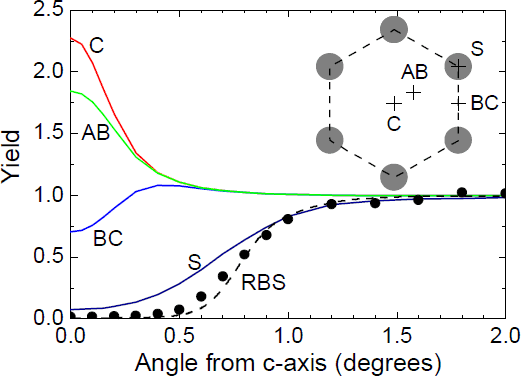
Figure 3 Solid curves show simulated NRA channeling yields for the various D lattice locations indicated in the inset. The dots and dashed curve show measured and simulated yields for 2MeV He4 scattered from host Ga atoms.
We have carried out computer simulations of the yield versus angle for various D locations in the GaN lattice. These simulations were done using a statistical equilibrium continuum (SEC) model [Reference Bech-Nielsen17] modified for the case of channeling along the c axis in wurtzite GaN. Our calculations use Doyle Turner potentials [Reference Doyle and Turner18] for the GaN lattice with 24 rows. The model includes dechanneling due to thermal vibration of the host atoms. RMS vibrational amplitudes of 0.00735 nm for Ga and 0.00806 nm for N were used [Reference Yoshiasa, Koto, Maeda and Ishii19]. The SEC model gave good agreement with the observed channeling dip for 2 MeV 4He backscattered from host lattice Ga as shown in figure 3, providing an important validation of the model. Figure 3 shows the NRA yield predicted by the SEC model for various locations of D in the channel as indicated in the inset diagram. Curve C is for D at the channel center, curve S is for D in-line with the host atom rows which includes BCN∥ sites. Curve AB is for D 0.056 nm from the channel center, corresponding to the ABMg-N⊥site. Also shown is the yield for D midway between the Ga and N atoms at the channel edge. D vibrational amplitudes used in the simulations (0.026 nm for BCN∥ and 0.018 nm for ABN⊥ and other sites) were estimated assuming a harmonic oscillator model with vibrational frequencies from the density functional calculations [Reference Myers3]. The D vibrational amplitude is mainly due to the low frequency bending modes. Except for the S site, changes in D vibrational amplitude by factors of 2 do not significantly change the calculated yield curves. The channeling simulations show that D near the channel center (which includes ABN⊥ sites) gives a narrow peak in the channeling yield and D along the host atom rows gives a broad dip. D at the channel edge midway between host atom rows gives a dip which is narrower and shallower.
The channeling results for the gas charged sample show that the D occupies at least two different sites. The narrow peak shows that 10-20% of the D is near the center of the trigonal channel. This peak is consistent with D at the ABMg-N⊥ site predicted by density functional theory for D+ passivating Mg acceptors, but could also be from neutral D0 or interstitial D2 which are also predicted to occupy sites near the channel center. In addition to the narrow peak there is a broad dip in channeling yield which shows that ∼30% of the D is at a different site near the rows of host atoms along the c direction. This may be D in the activated state whose configuration is not known. D is expected to be in this activated state during the channeling measurements due to electronic excitation by the analysis ion beam.
The two plasma charged samples have D concentrations exceeding the Mg concentration. Solubility calculations show that such high D concentrations indicate very high D chemical potentials [Reference Myers3]. One of the plasma charged samples shows a broad channeling dip similar to the gas charged sample, which may again be due to D in the activated state. This broad dip is not seen in the second plasma charged sample with the highest D concentration. The absence of channeling features in this sample indicates the D is incoherent with the GaN lattice, possibly due to precipitation or formation of extended defects induced by the very high D chemical potential. The absence of a narrow peak in both plasma charged samples shows that little of the D is localized near the channel center which rules out the presence of significant amounts of neutral D0, D2 or D+ passivating Mg. Finally, we observe that high off-axis ion beam doses cause a change in D location presumably due to production of lattice defects by collisional displacements.
Acknowledgements
This work was supported by the U.S. Department of Energy under contract DE-AC04-94AL85000, primarily under the auspices of the Office of Basic Energy Sciences.