


This article was received on Friday, June 19, 1998 and accepted on Thursday, September 10, 1998.
1. Introduction
Controllable doping is a key issue for the fabrication of ultraviolet and blue emitters based on GaN alloys. Si and Ge have been successfully used for n-type doping Reference Nakamura, Mukai and Senoh[1]. P-type doping remains a challenge because of the high n-type residual background present in GaN, and the large ionization energy of acceptors (Mg, Zn, Cd) Reference Strite and Morkoç[2]. P-type GaN has been achieved by Mg doping of metalorganic chemical vapor deposition (MOCVD) Reference Nakamura, Mukai, Senoh and Iwasa[3] and molecular beam epitaxy (MBE) Reference Kim, Salvador, Botchkarev, Aktas, Mohammad and Morcoc[4] layers. However, the large ionization energy of Mg (250 meV) Reference Pankove and Hutchby[5] implies a low activation of the acceptor at room temperature. Hence, the search for shallower acceptors is still a matter of great importance.
Be should be a shallower acceptor in GaN than Mg Reference Orton[6] Reference Podor[7] due to its large electronegativity and the absence of d-electrons Reference Strite[8]. Theoretical calculations suggest that Be behaves as a rather shallow acceptor in GaN Reference Park and Chadi[9], with a thermal ionization energy of 60 meV Reference Bernardini, Fiorentini and Bosin[10]. Nevertheless, experimental evidences point to the introduction of deep levels by Be doping in GaN. Several authors have reported a Be-related deep emission detected by photoluminescence (PL) in Be-doped Reference Ilegems and Dingle[11] Reference Cheng, Foxon, Jenkins, Hooper, Lacklison, Orton, Ber, Merkulov and Novikov[12] and Be-implanted GaN Reference Pankove and Hutchby[5], probably associated with the formation of complex defects. Salvador et al. Reference Salvador, Kim, Aktas, Botchkarev, Fan and Morkoc[13] observed a broad band centered at 390-420 nm, which is interpreted as a donor-acceptor emission involving Be acceptors, with an ionization energy of 250 meV.
In this work, the optical properties of GaN:Be layers will be analyzed in order to determine the shallow acceptor level and study the generation of deep levels.
2. Experimental
Be-doped wurtzite GaN layers were grown on Si (111) substrates by MBE in a MECA-2000 chamber Reference Sanchez-Garcia, Calleja, Sánchez, Calle, Monroy, Basak, Muñoz, Villar, Sanz-Hervás, Aguilar, Serrano and Blanco[14]. Nitrogen was supplied by an Oxford Applied Research RF plasma source, and high-purity ( ≥ 7N) standard solid sources were used for Ga and Be. Samples consist of an AlN buffer layer (500 Å) and a 0.5-1 μm thick GaN:Be layer grown at 840 °C and 750 °C respectively. The Be doping level was controlled varying the Be cell temperature (TBe) in the range of 700-910°C. Secondary ion mass spectroscopy (SIMS) measurements showed Be concentration increasing over two orders of magnitude in the TBe range of 700 − 870°C (Figure 1). The scale of Be concentration is arbitrary, because no SIMS calibration was available for Be in GaN.

Figure 1. Arrhenius plot of the Be concentration measured by SIMS as a function of the Be cell temperature. The scale of Be concentration is arbitrary, because no SIMS calibration was available for Be in GaN.
PL experiments were carried out in a He closed-cycle cryostat at temperatures between 4 and 300 K. The 334 nm line of an Ar+ laser was used for continuous wave (cw) excitation. Sample luminescence was dispersed by a THR-1000 Jobin-Yvon monochromator and detected by a GaAs photomultiplier. Time resolved PL measurements were performed at 10 K using a frequency doubled Ti-Sapphire laser with 200 fs pulses (peak power ∼ 0.2 MW/cm2 ) pumped by a mode-locked Ar+ laser, with a system time resolution of 100 ps.
PL detected electron paramagnetic resonance (PL-EPR) measurements were performed at 1.5 K, with a microwave frequency of 72 GHz (V-band), for higher resolution. The optical excitation was performed with a halogen lamp followed by a monochromator, and the magnetic resonance was measured as a change of the PL intensity detected by a photomultiplier, with amplitude modulation of the microwaves and lock-in techniques.
3. Results
A typical low temperature PL spectrum of a Be-doped GaN layer is shown in Figure 2. A narrow emission attributed to free excitons recombination is observed at 3.466 eV. In addition, new peaks at lower energies are present, related to transitions involving Be shallow acceptors Reference Dewsnip, Andrianov, Harrison, Orton, Lacklison, Ren, Hooper, Cheng and Foxon[15], as described below. A broad band centered at 2.4-2.5 eV is also observed as previously reported Reference Pankove and Hutchby[5] Reference Ilegems and Dingle[11] Reference Cheng, Foxon, Jenkins, Hooper, Lacklison, Orton, Ber, Merkulov and Novikov[12], with its emission shape modulated by a Fabry-Perot interference pattern. The integrated PL intensity of the band increases with Be doping level, whereas this emission is not detected in undoped samples. Hence, a relationship between this band and deep levels generated by Be will be established.

Figure 2. Typical low temperature PL spectrum of a Be-doped GaN layer.
3.1 The 3.466 eV line
The peak at 3.466 eV (15 meV full width half maximum, FWHM) observed in all samples is attributed to free excitons recombination (FXA), as deduced from the temperature evolution (4-300 K) shown in Figure 3, and time resolved PL spectra shown below. The effect of lattice vibrations on bandgap energy of semiconductors has been studied by Fan Reference Fan[16], who propose the following temperature dependence:

where E(0), θE, and κ are respectively the transition energy at 0 K, the Einstein temperature and a constant. The values obtained for these parameters with the best fit are: E(0) = 3.4658 ± 0.0001 eV, 0.171 ± 0.007 eV and θE = 447 ± 9 K. Calle et al. observed the FXA recombination at 3.479 eV in relaxed samples grown on Si (111) Reference Calle, Sanchez, Tijero, Sanchez-Garcia, Calleja and Berenford[17]. However, in the samples analyzed in this work, the energy position of FXA is affected by biaxial tensile strain due to thermal expansion mismatch between GaN and Si Reference Chichibu, Azuhata, Sota, Amano and Akasaki[18]. From x-ray diffraction measurements performed in these layers, a lattice parameter c = 5.1844 Å has been obtained, in agreement with the results by Chichibu et al. Reference Chichibu, Azuhata, Sota, Amano and Akasaki[18].

Figure 3. Temperature evolution of the transition energy of the near bandgap emissions. The best fit to the FXA variation and the fitting parameters are shown.
3.2 The 3.384 eV band
At lower energies than the FXA, Be-doped samples present a new emission (30 meV, FWHM) centered at 3.384 ± 0.001 eV, together with other recombinations at 3.292 and 3.202 eV. The energy spacing between these emissions (92 meV) reveals that the lower energy transitions are respectively the first and second LO phonon replicas of the luminescence at 3.384 eV. This recombination and its LO phonon replicas have been also recently observed on GaN layers grown by MBE on sapphire substrates Reference Dewsnip, Andrianov, Harrison, Orton, Lacklison, Ren, Hooper, Cheng and Foxon[15].
The variation of the energy position of the emissions with excitation power and temperature has been analyzed to identify the origin of the emission at 3.384 eV. Figure 4 shows the evolution of this transition with increasing temperature in the range 4-60 K. A blueshift of ∼ 4 meV is observed. This variation in the energy position corresponds to a rate of ~ k, the Boltzmann constant, consistent with that expected for a donor-acceptor pair recombination (DAP). This dependence with temperature is due to the enhancement of more closely spaced pairs by a higher thermal ionization rate for the donors Reference Lagerstedt and Monemar[19]. The evolution of the energy of the transition at 3.292 eV with increasing temperature is parallel to that described for the DAP band (Figure 3), supporting the identification of this emission as a first order LO phonon replica (DAP-LO).

Figure 4. Variation of PL spectra with increasing temperature under P = 1mW.
The evolution of the transition at 3.384 eV with increasing excitation power is depicted in Figure 5. The emission shifts 15 meV to higher energies when increasing the incident excitation power for almost three orders of magnitude (0.02-10 mW), what is consistent with the saturation of distant pairs under increasing excitation expected for a DAP recombination. On the contrary, the emission at 3.466 eV does not shift with excitation power, confirming its excitonic origin (FXA), as previously established.
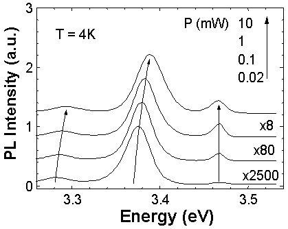
Figure 5. Evolution of PL spectra with increasing excitation power at T = 4K.
PL intensity decay measurements also support that the peak at 3.384 eV is a DAP transition. Figure 6 shows a comparison between the luminescence decays of the 3.466 eV emission (FXA) and that of the 3.384 eV peak (DAP). The excitonic emission shows a very fast and exponential decay, with a time constant limited by the system resolution (∼100 ps). Conversely, the decay of the DAP luminescence is slow and strongly non exponential, with a life time of 0.2 μs in the region between 200 ns and 500 ns.

Figure 6. Low temperature PL decays of FXA and DAP emissions.
Time resolved PL spectra are shown in Figure 7, recorded in several 10 ns periods from the beginning of the decay. The DAP emission and its first LO phonon replica shift to a lower energy (longer wavelength) with time. This red-shift is explained considering the exponential decrease of the transition probability with increasing distance between donor and acceptor. Thus, the recombination of close pairs (higher energy transitions) dominates the emission for short times (0-10 ns). On the contrary, the recombination of distant pairs (lower energy) becomes dominant at longer times (250-260 ns).
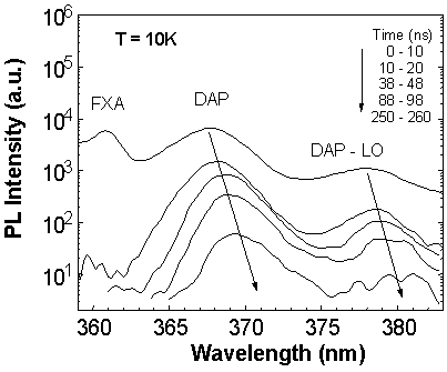
Figure 7. Time resolved PL spectra recorded in 10 ns periods between 0 and 260 ns at 10K.
All the above results are consistent with the identification of the peak at 3.384 eV with a DAP transition, with the acceptor probably related to substitutional Be. The energy of a DAP transition is given by:
The donor is likely the residual donor reported on our samples Reference Calle, Sanchez, Tijero, Sanchez-Garcia, Calleja and Berenford[17], with an ionization energy ED = 35 meV. The bandgap energy is reduced to Eg ≈ 3.492 eV because of the biaxial tensile strain Reference Chichibu, Azuhata, Sota, Amano and Akasaki[18], as was established for the FXA recombination. The coulombic interaction energy can be estimated as Ecoul ≈ 15 meV Reference Lagerstedt and Monemar[19]. Hence, an ionization energy EA ∼ 90 meV is derived for the Be-acceptor. This result is in agreement with recent theoretical calculations, predicting that Be is a shallow acceptor in GaN Reference Park and Chadi[9], with a thermal ionization energy of 60 meV Reference Bernardini, Fiorentini and Bosin[10], and it is very close to the 85 meV calculated by Pödör for the hydrogenic acceptor in GaN Reference Podor[7]. This conclusion is also supported by the recent work by Dewsnip et al. Reference Dewsnip, Andrianov, Harrison, Orton, Lacklison, Ren, Hooper, Cheng and Foxon[15] where a DAP character related to substitutional Be is attributed to the 3.384 eV recombination, finding an optical ionization energy between 90-100 meV for the Be acceptor.
3.3 The 2.4-2.5 band
The low temperature spectrum of a Be-doped layer presents also a broad band centered at 2.4-2.5 eV (Figure 2). Figure 8 shows this emission for different samples with increasing TBe, i.e., Be concentration. A clear relation between the intensity of this band and the Be concentration is observed, suggesting that this band is associated with complex defects involving Be.

Figure 8. Intensity variation of the 2.4-2.5 eV band at low temperature with increasing Be concentration.
Figure 9 shows the variation of the band position with excitation power. The center of the interferencial pattern envelope of the band shifts about 400 meV to higher energies when increasing the power three orders of magnitude (0.01-10 mW). This blue-shift is much higher than that corresponding to a DAP transition between discrete levels (see Figure 5 for 3.384 eV DAP). This fact points to a transition involving a broad band of deep levels related to Be.

Figure 9. Low temperature evolution of the 2.4-2.5 eV band with increasing excitation power.
The evolution of this luminescence with increasing temperature is shown in Figure 10. The center of the emission envelope is red-shifted ∼ 300 meV for a temperature range of 4-290 K. This shift to lower energies is higher than that observed in Figure 3 for the free exciton recombination, FXA. This behavior also suggests the presence of a band of deep states whose occupation level changes with temperature, rather than a single DAP recombination.

Figure 10. Evolution of the 2.4-2.5 eV band with temperature under P = 1mW.
Time resolved PL has also been performed in this spectral region at low temperature (10 K). The time evolution of the intensity at 2.25 eV is shown in Figure 11. The decay is extremely slow and clearly non exponential, with a lifetime of 10 μs for the range 4-10 μs. This result provides additional support for the interpretation of this broad band as produced by deep levels with different lifetimes, making the decay strongly non exponential.
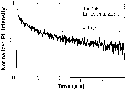
Figure 11. Low temperature PL decay of the emission at 2.25 eV.
PL-EPR measurements have been carried out in order to obtain more information about the levels involved in this transition. The PL-EPR spectrum shown in Figure 12 was measured via the 2.4-2.5 band. In first order perturbation theory, the deviation of the g factor from the free electron value, ge = 2.0023, is given by the expression:
where λ is the spin-orbit interaction constant, E is the energy of the perturbed state and E0 is the energy of the fundamental state, without perturbation effects. A donor-like resonance with a half width ∼ 7 mT was observed at 2.637 T (Figure 12), with an anisotropic g factor, g|| = 1.955 ± 0.001 and g⊥ = 1.949 ± 0.001 (|| and ⊥ indicate magnetic field B being parallel or perpendicular to the c-axis of the layers respectively). These results are in agreement with those obtained for the residual donor in undoped MOVPE layers grown on sapphire Reference Glaser, Kennedy, Doverspike, Rowland, Gaskill, Freitas, Asif Khan, Olson, Kuznia and Wickenden[20] Reference Koschnick, Michael, Spaeth, Beaumont, Gibart, Off, Sohmer and Scholz[21]. On the low field side of this resonance, there is another peak, with a half width ∼ 15 mT and g|| = 1.956 ± 0.001 and g⊥ = 1.957 ± 0.001 (inset in Figure 12), likely related to a second shallow donor also involved in the 2.4-2.5 eV luminescence. The resonance at lower magnetic field (2.57 T), with g = 2.008 ± 0.003, is assigned to an acceptor-like defect. This resonance does not present any anisotropy, as expected for a deep acceptor.

Figure 12. PL-EPR spectrum of a Be-doped GaN layer, measured via the 2.4-2.5 eV band. Inset : high resolution spectrum, showing shallow donors resonances.
All the experimental evidences described above suggest a model for the broad emission at 2.4-2.5 eV, that consists of a recombination between shallow residual donors, and a band of deep acceptors at 0.9−1 eV above the valence band.
4. Conclusions
PL spectra of Be-doped GaN samples are presented, and emissions at 3.466, 3.384 eV and a broad band at 2.4-2.5 eV have been studied. The transition at 3.466 eV is identified as a FXA recombination, as deduced from PL evolution with temperature and time resolved PL. The luminescence at 3.384 eV has been analyzed under cw excitation. PL measurements show blue-shifts with increasing temperature and excitation power. Time resolve PL experiments reveal a non exponential and slow decay, and a red-shift of the transition energy with time. These experimental evidences indicate a donor-acceptor origin, involving Be acceptors with an ionization energy as low as 90 meV. Hence, Be is confirmed as the shallowest acceptor reported in GaN. Finally, PL evolution with temperature, excitation power and time, together with PL-EPR measurements allow to associate the luminescence at 2.4-2.5 eV with a transition between shallow donors and a band of deep acceptors related to complex defects.
Acknowledgments
We would like to acknowledge Dr. A. Sanz Hervás and C. Villar for x-ray diffraction measurements and Dr. J. J. Serrano for SIMS analysis. This work has been partially supported by the European Union ESPRIT LTR contract LAQUANI 20968, the Acción Integrada 95-0188B and MAT 96-1947-CE.


