


Introduction
The use of nanowires as fillers in polymer nanocomposites can lead to materials with exceptional optical, electrical, mechanical, and thermal properties. Due to the high aspect ratio of the nanowires, a small number of nanowires can highly modify some of the physical properties of the polymeric matrix [e.g., conductivity (White et al., Reference White, Mutiso, Vora, Jahnke, Hsu, Kikkawa, Li, Fischer and Winey2010), dielectric constant (Liang et al., Reference Liang, Zhao, Hu and Sun2014), or thermal conductivity (Mi et al., Reference Mi, Li, Turng, Sun and Gong2014)], while leaving others almost intact (e.g., transparency, flexibility, or stretchability). This property enables the development of new materials, which present the combined properties (e.g., high dielectric constant and stretchability, conductivity and transparency, etc.) not available in single component materials. Applications of these novel materials include transparent electrodes for solar cell applications (Yu et al., Reference Yu, Li, Zhang, Hu and Pei2011; Zhang & Engholm, Reference Zhang and Engholm2018), flexible electrodes for wearable electronics (Langley et al., Reference Langley, Giusti, Mayousse, Celle, Bellet and Simonato2013; Li et al., Reference Li, Zhang, Shi, Xu, Qin, He, Yang, Dai, Liu, Zhou, Yu and Silva2020), and high dielectric constant or conductive stretchable materials for pressure and motion sensors (Wang et al., Reference Wang, Jiu, Nogi, Sugahara, Nagao, Koga, He and Suganuma2015; Jing et al., Reference Jing, Wang, Mi and Turng2019). Nanowire nanocomposite materials offer, in addition, the advantage of being solution processable (Gaynor et al., Reference Gaynor, Lee and Peumans2010; Zeng et al., Reference Zeng, Zhang, Yu and Lu2010) or printable (Nair et al., Reference Nair, Pakkathillam, Kumar, Arunachalam, Ray and Swaminathan2020; Wu et al., Reference Wu, Zhou, Wang and Li2020).
The macroscopic physical properties of nanowire nanocomposites depend critically on the distribution of the nanowires within the polymer matrix, and, specially, on the relative separation between nanowires. Information on the 2D distribution of nanowires in the plane of intact samples can be obtained by using different microscopy techniques, such as optical microscopy (restricted to transparent samples and with a lateral spatial resolution determined by the diffraction limit of light) or electron microscopy (with a spatial resolution affected by the insulating nature of the matrix). In order to determine the distribution in the vertical direction, nanoscale tomographic techniques, such as those based on electron microscopy or X-ray microscopy, would be necessary (Möbus & Inkson, Reference Möbus and Inkson2007; Withers, Reference Withers2007; Midgley & Dunin-Borkowski, Reference Midgley and Dunin-Borkowski2009). In practice, not many reports exist on the application of these nanotomographic techniques to nanowire composite materials (Englisch et al., Reference Englisch, Wirth, Schrenker, Tam, Egelhaaf, Brabec and Spiecker2018), due to their inherent difficulties when applied to polymeric materials. For this reason, alternative subsurface and nanotomographic techniques are under investigation. A range of these techniques are based on subsurface-sensitive scanning probe microscopy (SPM) techniques (Soliman et al., Reference Soliman, Ding and Tetard2017; Angeloni et al., Reference Angeloni, Reggente, Passeri, Natali and Rossi2018). Techniques such as scanning near-field ultrasound holography (Yamanaka & Ogiso, Reference Yamanaka and Ogiso1994; Shekhawat & Dravid, Reference Shekhawat and Dravid2005), mode synthesizing atomic force microscopy (AFM; Tetard et al., Reference Tetard, Passian and Thundat2010), multimodal AFM (Perrino et al., Reference Perrino, Ryu, Morales and Garcia2016), amplitude modulated AFM (Spitzer et al., Reference Spitzer, Riesch and Magerle2011), electrostatic force microscopy (Takano et al., Reference Takano, Wong, Harnisch and Porter2000; Jespersen & Nygard, Reference Jespersen and Nygard2007), scanning microwave impedance microscopy (Yang et al., Reference Yang, Lai, Tang, Kundhikanjana, Kelly, Zhang, Shen and Li2012; Gramse et al., Reference Gramse, Brinciotti, Lucibello, Patil, Kasper, Rankl, Hinterdorfer, Marcelli and Kienberger2015; Tselev et al., Reference Tselev, Velmurugan, Ievlev, Kalinin and Kolmakov2016), or scanning near-field optical microscopy (Govyadinov et al., Reference Govyadinov, Mastel, Gomar, Chuvilin, Carney and Hillenbrand2014) have shown all subsurface nanoscale imaging capabilities in polymeric nanocomposite materials.
Electrostatic force microscopy (EFM) is one of the subsurface SPM techniques that has experienced more progress toward its implementation as a nanotomographic technique for polymeric nanocomposite materials (Jespersen & Nygard, Reference Jespersen and Nygard2007; Castañeda-Uribe et al., Reference Castañeda-Uribe, Avila, Reifenberger and Raman2015; Cadena et al., Reference Cadena, Reifenberger and Raman2018; Fumagalli et al., Reference Fumagalli, Esfandiar, Fabregas, Hu, Ares, Janardanan, Yang, Radha, Taniguchi, Watanabe, Gomila, Novoselov and Geim2018; Fabregas & Gomila, Reference Fabregas and Gomila2020). Subsurface EFM imaging is based on the long-range nature of the electric forces, which can sense the presence and position of nanoscale objects buried within a polymeric material. Examples of subsurface imaging by EFM includes the detection of carbon nanotubes (Jespersen & Nygard, Reference Jespersen and Nygard2007; Zhao et al., Reference Zhao, Gu, Lowther, Park and Nguyen2010; Cadena et al., Reference Cadena, Misiego, Smith, Avila, Pipes, Reifenberger and Raman2013, Reference Cadena, Reifenberger and Raman2018; Thompson et al., Reference Thompson, Barroso-Bujans, Gomez-Herrero, Reifenberger and Raman2013; Castañeda-Uribe et al., Reference Castañeda-Uribe, Avila, Reifenberger and Raman2015; Patel et al., Reference Patel, Petty, Krafcik, Loyola, O'Bryan and Friddle2016), graphene networks (Alekseev et al., Reference Alekseev, Chen, Tkalya, Ghislandi, Syurik, Ageev, Loss and de With2012), and nanoparticles (Peng et al., Reference Peng, Zeng, Yang, Hu, Qiu and He2016) in polymer nanocomposites, of water-filled nanochannels buried in a van der Waals dielectric material (Fumagalli et al., Reference Fumagalli, Esfandiar, Fabregas, Hu, Ares, Janardanan, Yang, Radha, Taniguchi, Watanabe, Gomila, Novoselov and Geim2018) or of delta-doped layers in semiconductors (Gramse et al., Reference Gramse, Kölker, Škereň, Stock, Aeppli, Kienberger, Fuhrer and Curson2020). The subsurface and nanotomographic capabilities of EFM applied to nanowire nanocomposites have not been specifically analyzed. Some theoretical studies have been reported for the case of nanoparticles, carbon nanotubes, and thin-film nanocomposites (Jespersen & Nygard, Reference Jespersen and Nygard2007; Riedel et al., Reference Riedel, Alegria, Schwartz, Arinero, Colmenero and Saenz2011; Arinero et al., Reference Arinero, Riedel and Guasch2012; Castañeda-Uribe et al., Reference Castañeda-Uribe, Avila, Reifenberger and Raman2015; Fabregas & Gomila, Reference Fabregas and Gomila2020), but they have not addressed some key aspects relevant for nanowires nanocomposites, namely the achievable spatial resolution or the possibility to detect the capacitive coupling between nearby nanowires. Here, we develop a numerical approach to specifically investigate these aspects and demonstrate that quantitative EFM, which we refer to as scanning dielectric microscopy (SDM), can be a valuable nanoscopic technique for the nondestructive characterization of nanowire nanocomposites.
Materials and Methods
In SDM, an alternating electric potential of amplitude v 0 and frequency ω is applied between a conducting AFM cantilever probe and the conducting sample's substrate, with no mechanical oscillation applied (Fumagalli et al., Reference Fumagalli, Esteban-Ferrer, Cuervo, Carrascosa and Gomila2012; Fumagalli & Gomila, Reference Fumagalli, Gomila, Li and Ferrari2018). The excitation frequency is usually chosen smaller than the mechanical resonance frequency of the cantilever, ω 0, to prevent the influence of the mechanical response function of the cantilever. The applied voltage induces an electric force on the cantilever that depends quadratically on the applied voltage, so that force harmonics, and hence oscillation harmonics, at 0ω, ω, and 2ω appear. For dielectric measurements, the amplitude of the 2ω oscillation harmonic, A 2ω, is measured, from where the amplitude of the 2ω force harmonic, F 2ω, is obtained as F 2ω = kA 2ω, where k is the equivalent spring constant of the cantilever. The 2ω force harmonic amplitude, F 2ω, is directly related to the dielectric properties of the sample through the derivative of the capacitance with respect to the tip-sample distance, dC/dz (referred as to the capacitance gradient) by means of the relation F 2ω = 1/4dC/dz v 02. The quantitative analysis of the SDM measurements is performed by considering a realistic tip-sample geometrical model and solving for it Poisson's equation supplemented by the corresponding continuity and boundary conditions at the different surfaces and interfaces between different materials (Fumagalli et al., Reference Fumagalli, Esteban-Ferrer, Cuervo, Carrascosa and Gomila2012; Fumagalli & Gomila, Reference Fumagalli, Gomila, Li and Ferrari2018). The electric force is calculated by integration of the Maxwell stress tensor on the tip surface. The materials are usually characterized by its local relative dielectric constant, εr. At the usual low frequencies of the measurements (~kHz), conductivity effects can be modeled by considering a pure dielectric model with a very large dielectric constant value. It is worth noting that materials with even small conductivities appear as “metallic” for such low frequencies. In some specific setups, and by using the heterodyne detection method, very large frequencies, beyond the dielectric relaxation frequency of the material (typically in the GHz range) can be also considered (Gramse et al., Reference Gramse, Kölker, Škereň, Stock, Aeppli, Kienberger, Fuhrer and Curson2020). In these cases, the modeling needs to include explicitly the conductivity effects. In this case, materials will appear as “metallic” only when they display a significant conductivity. We do not consider this case in the present work (see, for instance, Gramse et al., Reference Gramse, Kölker, Škereň, Stock, Aeppli, Kienberger, Fuhrer and Curson2020). In the quantitative analysis, first the tip geometry is determined from electric force measurements made on a bare part of the conducting substrate by comparing them with the corresponding theoretically calculated electric forces, with the tip radius and half cone angle as fitting parameters. The local dielectric constant is determined from local electric force measurements made on the sample by comparing them to theoretically calculated electric forces with the local dielectric constant as a fitting parameter (Fumagalli et al., Reference Fumagalli, Esteban-Ferrer, Cuervo, Carrascosa and Gomila2012; Fumagalli & Gomila, Reference Fumagalli, Gomila, Li and Ferrari2018).
For the case of a single buried nanowire, we consider the model shown in Figure 1a. The nanowire is assumed to be cylindrical with diameter D w and length l w and be made of a lossless dielectric material with dielectric constant ε w (we model metallic nanowires by setting ε w very large, as mentioned above). The matrix of the nanocomposite material has thickness t m and dielectric constant ε m. The nanowire is located at a depth h, measured from the matrix surface to the upper edge of the nanowire. As in previous works (Fumagalli et al., Reference Fumagalli, Esteban-Ferrer, Cuervo, Carrascosa and Gomila2012; Gramse et al., Reference Gramse, Gomila and Fumagalli2012; Gomila et al., Reference Gomila, Gramse and Fumagalli2014), the probe consists of a conical tip of half angle θ and height H, ended by a tangent sphere of radius R and caped at the top with a disc cantilever of thickness W and radius H tanθ + L. Finally, the tip is located at a distance z from the matrix surface. The capacitance gradient, dC/dz, is obtained from the calculated electric force obtained by integration of the Maxwell stress tensor on the tip surface, as described above (Fumagalli et al., Reference Fumagalli, Esteban-Ferrer, Cuervo, Carrascosa and Gomila2012). All calculations have been done by using the electrostatic module of COMSOL MULTIPHYSICS 5.4 following similar methods to the ones described in the following publications (Lozano et al., Reference Lozano, Fabregas, Blanco-Cabra, Millán-Solsona, Torrents, Fumagalli and Gomila2018, Reference Lozano, Millán-Solsona, Fabregas and Gomila2019; Fabregas & Gomila, Reference Fabregas and Gomila2020).

Fig. 1. (a) Schematic representation of the model for a single buried nanowire, with the relevant parameters indicated. (b) Electric potential distribution across a cross-section of the sample for the tip at three different positions, X = 0, 100, and 200 nm. Parameters of the calculations: D w = 50 nm, l w = 1 μm, ε w = 104 (metallic), h = 10 nm, t m = 210 nm, ε m = 4, R = 100 nm, θ = 25°, H = 12.5 μm, W = 3 μm, L = 0 μm, z = 20 nm. (c) (symbols) Capacitance gradient (electric force) contrast profile ΔC′(X) at z = 20 nm. (continuous and dashed red lines) Fits to the numerically calculated profile with the modified Lorentzian function in equation (1) and with a Lorentzian with an offset, respectively. The fitted parameters are here  $\Delta {C}^{\prime}_0$ = 42.3 ± 0.1 zF/nm, w 0 = 149.5 ± 0.8 nm, and w 2 = 268 ± 1. nm.
Results
Capacitance Gradient Nanowire Spread Function
Figure 1b shows an example of the distribution of the electric potential along a cross section of the sample for three positions of the tip during a scan over the nanowire (X = 0, 100, and 200 nm). The nanowire is assumed to be metallic with diameter D w = 50 nm buried at a depth h = 10 nm in a matrix of thickness t m = 210 nm and with dielectric constant ε m = 4. The tip-sample distance and the tip radius are z = 20 nm and R = 100 nm, respectively (for the rest of tip parameters, see caption of Fig. 1). The electric potential distribution changes significantly when the tip passes over the nanowire, and so will the electric force acting on the tip, thus indicating that the tip can feel the presence of the buried nanowire. Figure 1c (symbols) shows the calculated tip-sample capacitance gradient contrast, ΔC′(X), as a function of the lateral position of the tip. The shape of the capacitance gradient contrast, ΔC′(X), looks similar to the one displayed by nonburied carbon nanotubes, which in Kalinin et al. (Reference Kalinin, Bonnell, Freitag and Johnson2002) was approximated by a Lorentzian function with an offset (three parameters function). Indeed, this function provided a good fit (R 2 ~ 0.997) to the calculated profiles (dashed line in Fig. 1c), but we observed some systematic deviations at the tails of the profiles. Since the spatial resolution analysis depends critically on the properties of these tails, we looked for a better capacitance gradient response function. We have verified that the upper part of the capacitance gradient contrast profile, ΔC′(X), shows a Lorentzian shape, like for carbon nanotubes (Kalinin et al., Reference Kalinin, Bonnell, Freitag and Johnson2002), but the decay of the lower part can be well approximated by a cubic function. To account for these two behaviors, an improved capacitance gradient nanowire spread function has been defined by modifying the Lorentzian function with a cubic decay
 $$\Delta {C}^{\prime}( X) {\kern 1pt} = \left\{{\matrix{ {\displaystyle{{\Delta {{C}^{\prime}}_0} \over {4{( {X/w_0} ) }^2 + 1}}; \;} \hfill & {0 \le \vert X \vert \le ( w_1^3 /8w_0^2 ) } \hfill , \cr {\displaystyle{{\Delta {{C}^{\prime}}_0} \over {4{( {2\vert X \vert /w_1} ) }^3 + 1}}; \;} \hfill & {( w_1^3 /8w_0^2 ) \le \vert X \vert } \hfill .} } \right.$$
Equation (1) is also a three parameters function, like a Lorentzian with an offset. Here,  $\Delta {C}^{\prime}_0$ is the maximum capacitance gradient contrast of the ΔC′(X) profile, w 0 is the full width at half maximum, and w 1 is the full width at one-fifth of the maximum. The continuous red line in Figure 1c corresponds to a least square fitting of equation (1) to the numerically calculated profile, giving in this case $\Delta {C}^{\prime}_0$ = 42.3 ± 0.1 zF/nm, w 0 = 149.5 ± 0.8 nm, and w 2 = 268 ± 1 nm. The agreement between equation (1) and the numerically calculated profile is almost perfect (R 2 > 0.999). The excellent agreement between equation (1) and the calculated data suggest that there could exist some fundamental theoretical explanation for it, but we have not been able to find it. In the present work, equation (1) is used as a phenomenological function to accurately and simply parametrize the electrostatic interaction between the tip and a buried nanowire in SDM.
Figures 2a–2e (symbols) show the calculated ΔC′(X) profiles corresponding to varying, respectively, the tip-sample distance, z, the tip radius, R, the dielectric constant of the matrix, ε m, the depth of the nanowire, h, and dielectric constant of the nanowire, ε w. The continuous lines in Figures 2a–2e represent the fitted curves by using equation (1). The agreement is excellent in all situations. Figures 2e–2h show the dependence of the fitted parameters of the nanowire spread function ( $\Delta {C}^{\prime}_0$, in the left axis, and w 0 and w 1/2 in the right axis) as a function of the corresponding system parameter. The maximum contrast, $\Delta {C}^{\prime}_0$, decreases as a function of both the tip-sample distance, z, and depth position of the nanowire, h, following a similar rational function
 $$\Delta {C}^{\prime}_0( z) {\kern 1pt} = {\kern 1pt} \displaystyle{{a( 1 + bz) } \over {( 1 + cz + dz^2) }},$$
 $$\Delta {C}^{\prime}_0( h) {\kern 1pt} = {\kern 1pt} \displaystyle{{{a}^{\prime}( 1 + {b}^{\prime}h) } \over {( 1 + {c}^{\prime}h + {d}^{\prime}h^2) }},$$
but with different coefficients (continuous lines in Figs. 2f, 2g, respectively). This type of decay is similar to the one observed for (nonburied) nanoparticles (Fumagalli et al., Reference Fumagalli, Esteban-Ferrer, Cuervo, Carrascosa and Gomila2012). Equations (2) and (3) are here used as phenomenological functions, which have been proposed by testing different functional dependences. In the present case, at tip-sample distances z > 100 nm or depths h > 150 nm, the tip practically does not feel anymore the presence of the nanowire. In addition,  $\Delta {C}^{\prime}_0$ increases roughly linearly with the tip radius, ~R (Fig. 2h); it shows a maximum as a function of the matrix dielectric constant at ε m ~ 4 and then decreases nearly logarithmically with ε m, ~log(ε m), until it approaches ~0 for ε m > 100 (Fig. 2i); and it increases logarithmically with ε w, ~log(ε w) for εw < 10 and then saturates to a constant value for εw > 104, which corresponds to the “metallic” limit (Fig. 2j). Concerning the widths w 0 and w 1, they both present a similar behavior. First, they increase (profile broadening) as the tip-sample distance or depth increases (Figs. 2f, 2g). Moreover, they increase as the tip radius increases (tip convolution) (Fig. 2h). Finally, they are relatively insensitive to the permittivity of the matrix and of the nanowire (Figs. 2i, 2j).

Fig. 2. (a–e) Constant height capacitance gradient profiles, ΔC′(X), at a tip-sample distance z = 20 nm for different tip-sample distances, z, depths, h, tip radii, R, matrix dielectric constants, ε m, and nanowire dielectric constants, ε w, respectively. Symbols correspond to the numerical calculations and the lines to least square fittings with the capacitance gradient nanowire spread function in equation (1). Parameters of the calculations, if not otherwise stated, same as those in Figure 1. (f–j) Dependence of the fitted parameters ( $\Delta {C}^{\prime}_0$, w 0, and w 1) on the system parameters corresponding to (a–e), respectively. The error bars represent the standard deviation of the fitted parameter. In (f) and (g), the continuous lines represent a phenomenological fit with a rational function of the form in equations (2) and (3), respectively. The fitted parameters are a = 166 zF/nm, b = −2.4 × 10⁻³ nm−1, c = 48 × 10−3 nm−1, and d = 45 × 10−3 nm−2 in (f) and a′ = 48 zF/nm, b′ = 6.0 × 10⁻⁴ nm−1, c′ = 11 × 10−3 nm−1, and d′ = 0.5 × 10⁻³ nm−2 in (g).
Spatial Resolution
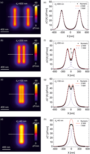
In order to investigate the achievable spatial resolution in SDM imaging, we have built a model like the one in Figure 1a but including two parallel nanowires. Figures 3a–3d show the constant height SDM images calculated for two nanowires buried at depths h 1 = h 2 = 10 nm and separated distances d w = 600, 200, 100, and 40 nm, respectively (the distances are measured from edge to edge of the nanowires). The parameters defining the nanowires, matrix and tip are the same as in Figure 1. For relatively large separations (d w > 100 nm, Figs. 3a–3c), the two nanowires can be well resolved in the SDM images (see also cross-section profiles, symbols, in Figs. 3e–3g). However, at a separation somewhere between ~100 and ~40 nm (Figs. 3d, 3h, symbols), the two nanowires cannot be resolved anymore. In order to determine theoretically the separation at which this happens, we performed calculations at more separations until the critical separation at which the nanowires cannot be resolved was determined. Figure 4a (symbols) shows the dependence of the difference between the maximum of the signal and the minimum in between the two nanowires, Δ (see Fig. 3f) as a function of the separation between the nanowires, d w, as determined from the capacitance gradient profiles numerically calculated for the two nanowire model, ΔC′(X). The spatial resolution,  $d_{\rm w}^\ast$, can be defined as the edge-to-edge nanowire separation for which Δ is at least twice the noise of the measuring instrument $\delta {C}^{\prime}_{{\rm noise}}$, that is, Δ = 2 × $\delta {C}^{\prime}_{{\rm noise}}$ (with $\delta {C}^{\prime}_{{\rm noise}}$ ~ 0.1–1 zF/nm, typically). From the data in Figure 4a, one gets $d_{\rm w}^\ast$ ~ 50 and 60 nm for noise levels of $\delta {C}^{\prime}_{{\rm noise}}$ = 0.1 and 1 zF/nm, respectively. The spatial resolution for other set of system parameters can be calculated in a similar way. However, determining the spatial resolution by performing multiple nanowire calculations, it is very time and computationally consuming. A much less costly approach can be used based on the capacitance gradient nanowire spread function [equation (1)]. Indeed, we note that the capacitance gradient cross-section profiles, ΔC′(X), for two nanowires in Figures 3e–3h can be reasonably well approximated by the sum of the single nanowires spread functions (red continuous line in Figs. 3e–3h),
 $$\Delta {C}^{\prime}_{2{\rm w}}( {X, \;d_{\rm w}} ) {\kern 1pt} = {\kern 1pt} \Delta {C}^{\prime}\left({X-\displaystyle{{d_{\rm w}} \over 2}-R_{\rm w}} \right) + \Delta {C}^{\prime}\left({X + \displaystyle{{d_{\rm w}} \over 2} + R_{\rm w}} \right).$$
Fig. 3. (a–d) Calculated constant height dC/dz EFM images for two parallel nanowires buried a depth h 1 = h 2 = 10 nm and separated distances d w = 600, 200, 100, and 40 nm, respectively. The parameters of the calculations are the same as in Figure 1. (e–h) (symbols) ΔC′(X) profiles calculated along the dashed lines shown in (a–d). The blue dashed lines and the continuous red lines represent, respectively, the capacitance gradient spread function of the individual nanowires [equation (1)] and of its addition [equation (4)].
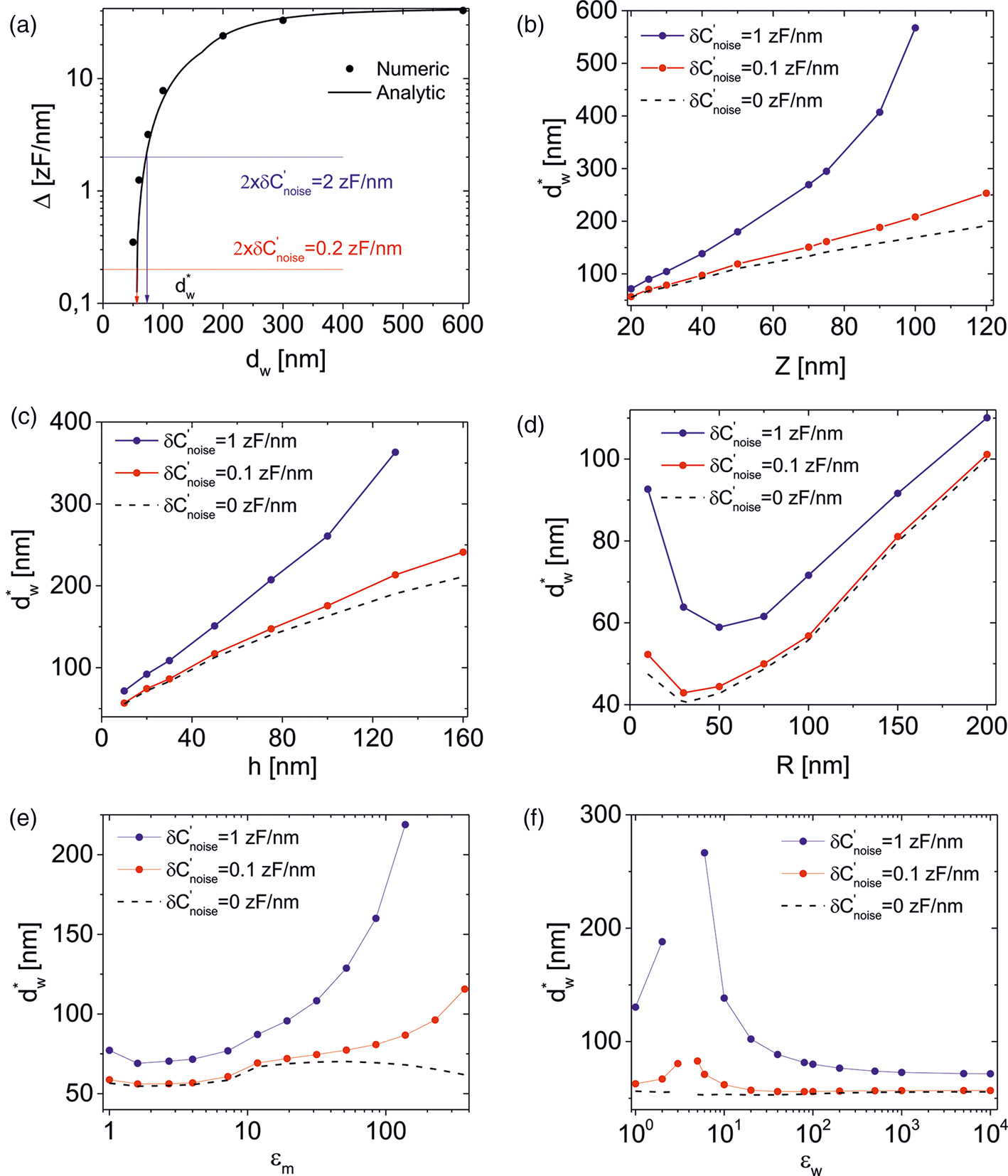
Fig. 4. (a) (symbols) Difference between one of the maxima and the minimum, Δ, of the calculated profiles ΔC′(X) in Figures 3e–3h, as a function of the separation between the nanowires (two additional separations d w = 60 and 70 nm are also considered). (continuous line) Approximation for Δ obtained from equation (5). The intersection of the curves with twice the noise levels, 2 ×  $\delta {C}^{\prime}_{{\rm noise}}$, gives the attainable spatial resolution, $d_{\rm w}^\ast$. (b–f) Spatial resolution for three noise levels ( $\delta {C}^{\prime}_{{\rm noise}}$ = 1 zF/nm, black symbols, 0.1 zF/nm, red symbols, and 0 zF/nm dashed line) as a function of, respectively, the tip-sample distance, z, depth, h, tip radius, R, matrix dielectric constant, ε m, and nanowire dielectric constant, ε w. The spatial resolution has been obtained by using equation (5) with the parameters ( $\Delta {C}^{\prime}_0$, w 0, and w 1) plotted in Figures 2f–2j.
The agreement is almost perfect when the nanowires are far apart (d w > 200 nm), and reasonably good until the nanowires are resolvable (for the smaller separations, a relevant discrepancy is observed related to the capacitive coupling of the nanowires, as will be discussed later). By assuming that the maxima is located at the position of the nanowires (e.g., X = d w/2+R w) and the minimum is at X = 0 one has from equation (4)
 $$\eqalign{\Delta & = \Delta {{C}^{\prime}}_{2{\rm w}}\left({\displaystyle{{d_{\rm w}} \over 2} + R_{\rm w}, \;d_{\rm w}} \right)-\Delta {{C}^{\prime}}_{2{\rm w}}( 0, \;d_{\rm w}) \cr & = \Delta {C}^{\prime}( 0 ) + \Delta {C}^{\prime}( d_{\rm w} + 2R_{\rm w}) -2\Delta {C}^{\prime}\left({\displaystyle{{d_{\rm w}} \over 2} + R_{\rm w}} \right),} $$
where in the second line we used equation (1). Equation (5) enables calculating the parameter Δ from the single nanowire spread function and its parameters ( $\Delta {C}^{\prime}_0$, w 0, and w 1). The solid line in Figure 4a shows the prediction from equation (5). The agreement with the numerically calculated values corresponding to the two nanowire model (symbols) is very good. We note that the good agreement is maintained even if the values of the maxima and minimum themselves are affected by the capacitive coupling. Therefore, a good estimation of the spatial resolution can be obtained from equation (5) and the single nanowire spread function and its parameters ( $\Delta {C}^{\prime}_0$, w 0, and w 1), without the need to perform complex and long multiple nanowire calculations. We note that the value of the minimum spatial resolution deduced from this analysis ( $d_{\rm w}^\ast$ ~ 50 nm) is smaller than half the full width at half maximum of the spread function (w 0/2 = 75 nm), which is sometimes used to estimate the spatial resolution in SDM measurements (Cadena et al., Reference Cadena, Reifenberger and Raman2018). Figures 4b–4f show the spatial resolution calculated in this way for three instrumental noise values, $\delta {C}^{\prime}_{{\rm noise}}$ = 1 zF/nm (blue symbols), 0.1 zF/nm (red symbols), and 0 zF/nm (dashed line, ultimate limit), as a function of the tip-sample distance, depth, tip radius, matrix dielectric constant, and nanowire dielectric constant, respectively. The calculations have been done by using the fitted parameters in Figure 2. We first note that for shallow buried nanowires (at depths smaller than ~40 nm), sub-100 nm spatial resolution is relatively easily achievable if SDM images are acquired at close distances from the surface of the matrix (below ~40 nm). The specific spatial resolution attainable depends on the system parameters. For instance, in the present case, the optimum spatial resolution can be achieved by considering intermediate tip radius values (here R ~ 40−50 nm, see Figure 4d, commensurate with the nanowire diameter), rather than considering very small tip radius. One reason being that the cone contribution in the imaging of buried nanowires plays a relevant role, so that a larger radius makes the cone contribution to be slightly smaller than for a small tip radius (since then the cone will be closer to the surface). Another reason is that the capacitive coupling between tip and nanowire is optimal when they have similar diameters. When the nanowires are buried deeper than some tens of nanometers, the spatial resolution increases roughly linearly with the depth (Fig. 4c), the faster the decrease, the larger the instrumental noise. Surprisingly enough the dielectric constant of the matrix does not play a big role in a relatively broad range of values 1 < ε m < 20 (Fig. 4e), due to the relatively little dependence of the widths of the nanowire spread function on this parameter (Fig. 3i). For large ε m values, the spatial resolution is larger due to the screening of the electric potential by the matrix and the reduction of the maximum contrast (Fig. 3i). The dependence on the dielectric constant of the nanowires, ε w, is similar to that on ε m, except for values close to the matrix dielectric constant (here ε w = 4), where it decreases largely due to the loss of dielectric contrast when the nanowire dielectric constant equals that of the matrix (Fig. 2j). As a rule, any parameter either reducing the maximum contrast or increasing the widths of the nanowire spread function (or both) will result in a decrease in the attainable spatial resolution.
Nanowire Capacitive Coupling
We have seen in Figures 3e–3h that the numerically calculated capacitance gradient contrast profiles, ΔC′(X), depart at small separations (d w < 100 nm) from the ones calculated by just adding the nanowire spread functions of the individual nanowires [equation (4)]. As we have mentioned before, this fact is due to the capacitive coupling between the nanowires, which makes that some electrostatic energy of the system is stored in between the nanowires, thus reducing the electrostatic force acting on the tip as compared with the value that would be obtained with just the addition of the forces made by each individual nanowire. The relevance of the capacitive coupling can be estimated from the capacitance per unit of length between two long parallel nanowires in an infinite medium with dielectric constant ε m given by (Smythe, Reference Smythe1968)
 $$c_{2NW} = \displaystyle{{\pi \varepsilon _0\varepsilon _{\rm m}} \over {{\cosh }^{{-}1}( {1 + ( d_{\rm w}/D_{\rm w}) } ) }}.$$
This function increases sharply for d w < D w, meaning that in this range of separations, the capacitive coupling is relevant. This result coincides with that observed from the two nanowire numerical calculations in Figure 3. Since the capacitive coupling between nanowires affects the electrostatic force acting on the tip, this implies that SDM measurements can be sensitive to the capacitive coupling between nanowires. This result is relevant since the overall dielectric properties of the nanocomposites are expected to be strongly dependent on the relevance of the capacitive coupling between nearby nanowires, which would determine a sort of dielectric percolative path, in as much the same way, as the conductive properties depend on the existence of percolative conductive paths (Kalinin et al., Reference Kalinin, Bonnell, Freitag and Johnson2002).
Discussion
We have analyzed the spatial resolution achievable in the subsurface characterization of nanowire nanocomposites by means of SDM. For a given nanowire nanocomposite, we have shown that the best spatial resolution can be achieved for the smallest possible measuring distances and by using a tip with a radius commensurate with the nanowire diameter. The spatial resolution is expected to be optimal for the nanowires close to the surface (at depths up to around the tip radius), but it will increase quickly as the depth increases. The instrumental noise of the measuring apparatus,  ${\rm \delta }{C}^{\prime}_{{\rm noise}}$, plays an important role in the performance of SDM as a subsurface characterization technique. Under optimal measuring conditions, the relevance of the instrumental noise is moderate (e.g., passing from an instrumental noise of 0.1 to 1 zF/nm increases the spatial resolution only by around a ~25–50%). However, under nonoptimal conditions (e.g., large tip-sample distances, noncommensurate tip radius, deep nanowires), the spatial resolution degrades quickly as the instrumental noise increases. Since optimal measuring conditions cannot be guaranteed in all situations, the instrumental noise turns out to be probably the more decisive parameter in subsurface SDM imaging. Based on this analysis, the best strategy to implement subsurface SDM imaging in nanowire nanocomposites is to choose a measuring probe with a tip radius commensurate to the diameter of the nanowires and with a cantilever with an equivalent spring constant small enough to allow for low noise measurements but high enough to allow performing measurements at close distances without jumping into contact with the sample (typically spring constants in the range ~0.1−0.5 N/m).
In its conventional use at low frequencies (~kHz), SDM is mainly applicable to nanocomposites with insulating matrices. Otherwise, if some conductivity exists, the matrix would appear as “metallic” at these frequencies and will strongly screen the applied electric field, loosing the subsurface imaging capabilities. To overcome this limitation, one can consider measurements at very high frequencies (f > GHz), beyond the dielectric relaxation frequency of the material, as we have discussed in the section “Materials and methods” (Gramse et al., Reference Gramse, Kölker, Škereň, Stock, Aeppli, Kienberger, Fuhrer and Curson2020). In this respect, it is worth remarking on the qualitative similarities that persist between measurements performed under such different imaging conditions on buried nanostructures (Gramse et al., Reference Gramse, Kölker, Škereň, Stock, Aeppli, Kienberger, Fuhrer and Curson2020). However, quantitatively, the differences can be remarkable since the actual electric force depends on the details of the systems, including the 3D geometry of the buried nano-object or measuring frequency, among others.
Compared with optical microscopy, SDM offers the advantage of being applicable to transparent and nontransparent nanocomposites, and to offer a spatial resolution well below the diffraction limit of light (~250 nm), even on nanowires buried hundreds of nanometers deep inside the nanocomposite. Compared with electron microscopy, SDM offers the advantage of being applicable in ambient conditions (or liquid and vacuum if required) and to insulating matrix nanocomposites without damaging the sample during imaging. In electron microscopy, to prevent beam damage when studying insulating materials, the experiments sometimes need to be performed at low temperatures or to make use of highly sensitive and expensive cameras. To determine the achievable spatial resolution and depth sensitivity that can be achieved with electron microscopy in this type of sample, as compared with SDM, a specific study would be required, since the insulating nature of the matrix could lead to severe shifts during the acquisition, which could largely degrade the usually very high spatial resolution achievable.
Conclusions
We have shown that SDM can be a valuable nondestructive nanoscopic technique for the subsurface characterization of nanowire nanocomposites. We have shown that the capacitance gradient nanowire spread function of an isolated buried nanowire consists of a modified Lorentzian with a cubic decay, and that this function can be used to easily predict the spatial resolution achievable in SDM subsurface imaging. The dependence of the spatial resolution on several system parameters has been analyzed. As a rule, we have demonstrated that any system parameter decreasing the maximum of the nanowire spread function or increasing, its widths (or both) will result in a loss of spatial resolution. In addition, the instrumental noise also plays a key role, specially when nonoptimal measuring conditions cannot be met. Based on this analysis, we have proposed an optimal measuring strategy. In addition, we have shown that SDM is also sensitive to the capacitive coupling between nearby nanowires when they are located at separations smaller than the diameter of the nanowires. This result opens the possibility to use SDM to detect the capacitive coupling between nearby nanowires in a nanowire nanocomposite, which is relevant for the determination of the overall dielectric properties of the material. The present results open the way to use SDM in the optimization of nanowire nanocomposite materials.
Funding
This work was partially supported by the Spanish Ministerio de Economıa, Industria y Competitividad and EU FEDER through Grant No. PID2019-111376RA-I00, the Generalitat de Catalunya through Grant No. 2017-SGR1079, and the CERCA Program. This work also received funding from the European Commission under Grant Agreement No. H2020-MSCA-721874 (SPM2.0). R.F. and L.F. received funding from the Marie Sklodowska-Curie Actions (Grant No. 842402, Dielec2DBiomolecules) and the European Research Council (Grant Agreement No. 819417, Liquid2DM) under the European Union's Horizon 2020 research and innovation program.


 Open access