Hostname: page-component-8448b6f56d-c4f8m Total loading time: 0 Render date: 2024-04-23T15:16:57.776Z Has data issue: false hasContentIssue false

Surface plasmon propagation on overcrossing metallic waveguides fabricated by a pick-and-place method

Published online by Cambridge University Press:  23 December 2015

Yusuke Nagasaki
Affiliation:
Graduate School of Engineering, Osaka University, 2-1 Yamadaoka, Suita, Osaka 565-0871, Japan
Masashi Miyata
Affiliation:
Graduate School of Engineering, Osaka University, 2-1 Yamadaoka, Suita, Osaka 565-0871, Japan
Mai Higuchi
Affiliation:
Graduate School of Engineering, Osaka University, 2-1 Yamadaoka, Suita, Osaka 565-0871, Japan
Junichi Takahara*
Affiliation:
Graduate School of Engineering, Osaka University, 2-1 Yamadaoka, Suita, Osaka 565-0871, Japan Photonic Advanced Research Center, Osaka University, 2-1 Yamadaoka, Suita, Osaka 565-0871, Japan
*
Address all correspondence to Junichi Takahara attakahara@ap.eng.osaka-u.ac.jp
Get access

Abstract

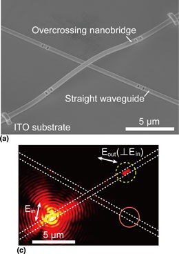
Plasmonic waveguides can transport light while still confining it beyond the diffraction limit. Recently, crossing plasmonic waveguides have been suggested for the implementation of higher-density optical networks. However, suppressing undesirable scattering at their crossing point is still a challenging task because waveguides in these structures are physically connected. Here, we present an experimental demonstration of surface plasmon propagation on an overcrossing metallic waveguide fabricated by a pick-and-place method. By spatially separating the waveguides, the undesirable interaction at the interconnection can be suppressed. Our approach could be a powerful platform to achieve high-density integration of optical waveguides.

Type
Plasmonics, Photonics, and Metamaterials Research Letters
Copyright
Copyright © Materials Research Society 2015 

Access options

Get access to the full version of this content by using one of the access options below. (Log in options will check for institutional or personal access. Content may require purchase if you do not have access.)

References

1. Takahara, J. and Kobayashi, T.: Low-dimensional optical waves and nano-optical circuits. Opt. Photonics News 15, 5459 (2004).Google Scholar
2. Brongersma, M.L., Schuller, J.A., White, J., Jun, Y.C., Bozhevolnyi, S.I., Sondergaard, T., and Zia, R.: Nanoplasmonics: components, devices, and circuits. In Plasmonic Nanoguides and Circuits, edited by Bozhevolnyi, S.I. (Pan Stanford Publishing, Singapore, 2009), 405438.Google Scholar
3. Barnes, W.L., Dereux, A., and Ebbesen, T.W.: Surface plasmon subwavelength optics. Nature 424, 824830 (2003).Google Scholar
4. Brongersma, M.L. and Shalaev, V.M.: The case for plasmonics. Science 328, 440441 (2010).Google Scholar
5. Miyata, M. and Takahara, J.: Excitation control of long-range surface plasmons by two incident beams. Opt. Express 20, 94939500 (2012).Google Scholar
6. Takahara, J., Yamagishi, S., Taki, H., Morimoto, A., and Kobayashi, T.: Guiding of a one-dimensional optical beam with nanometer diameter. Opt. Lett. 22, 475477 (1997).Google Scholar
7. Berini, P.: Plasmon–polariton modes guided by a metal film of finite width. Opt. Lett. 24, 10111013 (1999).Google Scholar
8. Veronis, G. and Fan, S.: Guided subwavelength plasmonic mode supported by a slot in a thin metal film. Opt. Lett. 30, 33593361 (2005).Google Scholar
9. Pile, D.F.P. and Gramotnev, D.K.: Channel plasmon–polariton in a triangular groove on a metal surface. Opt. Lett. 29, 10691071 (2004).Google Scholar
10. Xiao, S. and Mortensen, N.A.: Resonant-tunnelling-assisted crossing for subwavelength plasmonic slot waveguides. Opt. Express 16, 1499715005 (2008).Google Scholar
11. Li, Y., Xu, C., Zeng, C., Wang, W., Yang, J., Yu, H., and Jiang, X.: Hybrid plasmonic waveguide crossing based on the multimode interference effect. Opt. Commun. 335, 8689 (2015).Google Scholar
12. Ota, M., Fukuhara, M., Sumimura, A., Ito, M., Aihara, T., Ishii, Y., and Fukuda, M.: Dielectric-loaded surface plasmon polariton crossing waveguides using multimode interference. Opt. Lett. 40, 22692272 (2015).CrossRefGoogle ScholarPubMed
13. Manolatou, C., Johnson, S.G., Fan, S., Villeneuve, P.R., Haus, H.A., and Joannopoulos, J.D.: High-density integrated optics. J. Lightw. Technol. 17, 16821692 (1999).Google Scholar
14. Fukazawa, T., Hirano, T., Ohno, F., and Baba, T.: Low loss intersection of Si photonic wire waveguides. Jpn. J. Appl. Phys. 43, 646647 (2004).Google Scholar
15. Lindquist, N.C., Johnson, T.W., Norris, D.J., and Oh, S.-H.: Monolithic integration of continuously tunable plasmonic nanostructures. Nano Lett. 11, 35263530 (2011).Google Scholar
16. Miyata, M., Holsteen, A., Nagasaki, Y., Brongersma, M.L., and Takahara, J.: Gap plasmon resonance in a suspended plasmonic nanowire coupled to a metallic substrate. Nano Lett. 15, 56095616 (2015).Google Scholar
17. Wen, J., Banzer, P., Kriesch, A., Ploss, D., Schmauss, B., and Peschel, U.: Experimental cross-polarization detection of coupling far-field light to highly confined plasmonic gap modes via nanoantennas. Appl. Phys. Lett. 98, 101109 (2011).CrossRefGoogle Scholar
18. Johnson, P.B. and Christy, R.W.: Optical constants of the noble metals. Phys. Rev. B 6, 43704379 (1972).Google Scholar
19. Palik, E.D.: Handbook of Optical Constants of Solids. Academic Press, New York (1998).Google Scholar
20. Barnes, W.L.: Surface plasmon–polariton length scales: a route to sub-wavelength optics. J. Opt. A, Pure Appl. Opt. 8, S87S93 (2006).Google Scholar