Hostname: page-component-7c8c6479df-fqc5m Total loading time: 0 Render date: 2024-03-29T00:38:12.768Z Has data issue: false hasContentIssue false

Fabrication of nickel and nickel carbide thin films by pulsed chemical vapor deposition

Published online by Cambridge University Press:  26 February 2018

Qun Guo
Affiliation:
Laboratory of Plasma Physics and Materials, Beijing Institute of Graphic Communication, Beijing 102600, China
Zheng Guo
Affiliation:
School of Advanced Materials, Shenzhen Graduate School, Peking University, Shenzhen 518055, China
Jianmin Shi
Affiliation:
Institute of Nuclear Physics and Chemistry, China Academy of Engineering Physics, Mianyang 621000, China
Lijun Sang
Affiliation:
Laboratory of Plasma Physics and Materials, Beijing Institute of Graphic Communication, Beijing 102600, China
Bo Gao
Affiliation:
Laboratory of Plasma Physics and Materials, Beijing Institute of Graphic Communication, Beijing 102600, China
Qiang Chen
Affiliation:
Laboratory of Plasma Physics and Materials, Beijing Institute of Graphic Communication, Beijing 102600, China
Zhongwei Liu*
Affiliation:
Laboratory of Plasma Physics and Materials, Beijing Institute of Graphic Communication, Beijing 102600, China
Xinwei Wang*
Affiliation:
School of Advanced Materials, Shenzhen Graduate School, Peking University, Shenzhen 518055, China
*
Address all correspondence to Zhongwei Liu and Xinwei Wang at liuzhongwei@bigc.edu.cn; wangxw@pkusz.edu.cn
Get access

Abstract

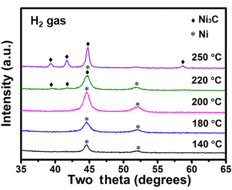
We report a new pulsed chemical vapor deposition (PCVD) process to deposit nickel (Ni) and nickel carbide (Ni3C x ) thin films, using bis(1,4-di-tert-butyl-1,3-diazabutadienyl)nickel(II) precursor and either H2 gas or H2 plasma as the coreactant, at a temperature from 140 to 250 °C. All the PCVD films are fairly pure with low levels of N and O impurities. The films deposited with H2 gas at ≤200 °C are faced centered cubic-phase Ni metal films with low C content; but at ≥220 °C, another phase of rhombohedral Ni3C is formed and the C content increases. However, when H2 plasma is used, the films are always in rhombohedral Ni3C phase for the entire temperature range.

Type
Research Letters
Copyright
Copyright © Materials Research Society 2018 

Access options

Get access to the full version of this content by using one of the access options below. (Log in options will check for institutional or personal access. Content may require purchase if you do not have access.)

Footnotes

*

Q.G. and Z.G. contributed equally to this work.

References

1. Kittl, J.A., Lauwers, A., Chamirian, O., Van Dal, M., Akheyar, A., De Potter, M., Lindsay, R., and Maex, K.: Ni- and Co-based silicides for advanced CMOS applications. Microelectron. Eng. 70, 158 (2003).CrossRefGoogle Scholar
2. Ha, J.-B., Yun, S.-W., and Lee, J.-H.: Effect of poly silicon thickness on the formation of Ni-FUSI gate by using atomic layer deposited nickel film. Curr. Appl. Phys. 10, 41 (2010).Google Scholar
3. Zavracky, P.M., Majumder, S., and McGruer, N.E.: Micromechanical switches fabricated using nickel surface micromachining. J. Microelectromech. Syst. 6, 3 (1997).Google Scholar
4. Kataoka, K., Kawamura, S., Itoh, T., Ishikawa, K., Honma, H., and Suga, T.: Electroplating Ni micro-cantilevers for low contact-force IC probing. Sens. Actuators A, Phys. 103, 116 (2003).Google Scholar
5. Teh, W.H., Luo, J.K., Graham, M.R., Pavlov, A., and Smith, C.G.: Near-zero curvature fabrication of miniaturized micromechanical Ni switches using electron beam cross-linked PMMA. J. Micromech. Microeng. 13, 591 (2003).CrossRefGoogle Scholar
6. Li, H., Shao, Y., Su, Y., Gao, Y., and Wang, X.: Vapor-phase atomic layer deposition of nickel sulfide and its application for efficient oxygen-evolution electrocatalysis. Chem. Mater. 28, 1155 (2016).CrossRefGoogle Scholar
7. Xiong, W., Guo, Q., Guo, Z., Li, H., Zhao, R., Chen, Q., Liu, Z., and Wang, X.: Atomic layer deposition of nickel carbide for supercapacitors and electrocatalytic hydrogen evolution. J. Mater. Chem. A doi: 10.1039/C7TA10202J (2018).Google Scholar
8. Yanguas-Gil, A., Yang, Y., Kumar, N., and Abelson, J.R.: Highly conformal film growth by chemical vapor deposition. I. A conformal zone diagram based on kinetics. J. Vac. Sci. Technol. A 27, 1235 (2009).Google Scholar
9. George, S.M.: Atomic layer deposition: an overview. Chem. Rev. 110, 111 (2010).Google Scholar
10. Meng, X., Wang, X., Geng, D., Ozgit-Akgun, C., Schneider, N., and Elam, J.W.: Atomic layer deposition for nanomaterial synthesis and functionalization in energy technology. Mater. Horiz. 4, 133 (2017).CrossRefGoogle Scholar
11. Xiong, W., Guo, Z., Li, H., Zhao, R., and Wang, X.: Rational bottom-up engineering of electrocatalysts by atomic layer deposition: a case study of FexCo1–xSy-based catalysts for electrochemical hydrogen evolution. ACS Energy Lett. 2, 2778 (2017).Google Scholar
12. Shao, Y., Guo, Z., Li, H., Su, Y., and Wang, X.: Atomic layer deposition of iron sulfide and its application as a catalyst in the hydrogenation of azobenzenes. Angew. Chem. Int. Ed. 56, 3226 (2017).CrossRefGoogle ScholarPubMed
13. Li, H., Guo, Z., and Wang, X.: Atomic-layer-deposited ultrathin Co9S8 on carbon nanotubes: an efficient bifunctional electrocatalyst for oxygen evolution/reduction reactions and rechargeable Zn–air batteries. J. Mater. Chem. A 5, 21353 (2017).Google Scholar
14. Li, H., Gao, Y., Shao, Y., Su, Y., and Wang, X.: Vapor-phase atomic layer deposition of Co9S8 and its application for supercapacitors. Nano Lett. 15, 6689 (2015).CrossRefGoogle ScholarPubMed
15. Gao, Y., Shao, Y., Yan, L., Li, H., Su, Y., Meng, H., and Wang, X.: Efficient charge injection in organic field-effect transistors enabled by low-temperature atomic layer deposition of ultrathin VOx interlayer. Adv. Funct. Mater. 26, 4456 (2016).CrossRefGoogle Scholar
16. Wang, X. and Gordon, R.G.: Smooth, low-resistance, pinhole-free, conformal ruthenium films by pulsed chemical vapor deposition. ECS J. Solid State Sci. Technol. 2, N41 (2012).CrossRefGoogle Scholar
17. Wang, X. and Gordon, R.G.: High-quality epitaxy of ruthenium dioxide, RuO2, on rutile titanium dioxide, TiO2, by pulsed chemical vapor deposition. Cryst. Growth Des. 13, 1316 (2013).Google Scholar
18. Protopopova, V.S. and Alexandrov, S.E.: Mass-spectrometric and kinetic study of Ni films MOCVD from bis-(ethylcyclopentadienyl) nickel. Surf. Coat. Technol. 230, 316 (2013).Google Scholar
19. Yuan, G., Shimizu, H., Momose, T., and Shimogaki, Y.: Role of NH3 feeding period to realize high-quality nickel films by hot-wire-assisted atomic layer deposition. Microelectron. Eng. 120, 230 (2014).CrossRefGoogle Scholar
20. Wang, Y.-P., Ding, Z.-J., Liu, Q.-X., Liu, W.-J., Ding, S.-J., and Zhang, D.W.: Plasma-assisted atomic layer deposition and post-annealing enhancement of low resistivity and oxygen-free nickel nano-films using nickelocene and ammonia precursors. J. Mater. Chem. C 4, 11059 (2016).Google Scholar
21. Sarr, M., Bahlawane, N., Arl, D., Dossot, M., McRae, E., and Lenoble, D.: Tailoring the properties of atomic layer deposited nickel and nickel carbide thin films via chain-length control of the alcohol reducing agents. J. Phys. Chem. C 118, 23385 (2014).CrossRefGoogle Scholar
22. Utriainen, M., Kröger-Laukkanen, M., Johansson, L.-S., and Niinistö, L.: Studies of metallic thin film growth in an atomic layer epitaxy reactor using M(acac)2 (M = Ni, Cu, Pt) precursors. Appl. Surf. Sci. 157, 151 (2000).CrossRefGoogle Scholar
23. Premkumar, P.A., Bahlawane, N., and Kohse-Höinghaus, K.: CVD of metals using alcohols and metal acetylacetonates, part I: optimization of process parameters and electrical characterization of synthesized films. Chem. Vapor Depos. 13, 219 (2007).Google Scholar
24. Han-Bo-Ram, L., Sung-Hwan, B., Woo-Hee, K., Gil Ho, G., Young Kuk, L., Taek-Mo, C., Chang Gyoun, K., Chan Gyung, P., and Hyungjun, K.: Plasma-enhanced atomic layer deposition of Ni. Jpn. J. Appl. Phys. 49, 05FA11 (2010).Google Scholar
25. Li, Z., Gordon, R.G., Pallem, V., Li, H., and Shenai, D.V.: Direct-liquid-injection chemical vapor deposition of nickel nitride films and their reduction to nickel films. Chem. Mater. 22, 3060 (2010).Google Scholar
26. Lim, B.S., Rahtu, A., and Gordon, R.G.: Atomic layer deposition of transition metals. Nat. Mater. 2, 749 (2003).CrossRefGoogle ScholarPubMed
27. Kim, J., Jang, W., Park, J., Jeon, H., Kim, H., Yuh, J., and Jeon, H.: Characteristics of a nickel thin film and formation of nickel silicide by using remote plasma atomic layer deposition with Ni(iPr-DAD)2 . J. Korean Phys. Soc. 66, 821 (2015).CrossRefGoogle Scholar
28. Guo, Z., Li, H., Chen, Q., Sang, L., Yang, L., Liu, Z., and Wang, X.: Low-temperature atomic layer deposition of high purity, smooth, low resistivity copper films by using amidinate precursor and hydrogen plasma. Chem. Mater. 27, 5988 (2015).CrossRefGoogle Scholar
29. Goto, Y., Taniguchi, K., Omata, T., Otsuka-Yao-Matsuo, S., Ohashi, N., Ueda, S., Yoshikawa, H., Yamashita, Y., Oohashi, H., and Kobayashi, K.: Formation of Ni3C nanocrystals by thermolysis of nickel acetylacetonate in oleylamine: characterization using hard X-ray photoelectron spectroscopy. Chem. Mater. 20, 4156 (2008).CrossRefGoogle Scholar
30. Bayer, B.C., Bosworth, D.A., Michaelis, F.B., Blume, R., Habler, G., Abart, R., Weatherup, R.S., Kidambi, P.R., Baumberg, J.J., and Knop-Gericke, A.: In situ observations of phase transitions in metastable nickel (carbide)/carbon nanocomposites. J. Phys. Chem. C 120, 22571 (2016).CrossRefGoogle ScholarPubMed