Hostname: page-component-77c89778f8-sh8wx Total loading time: 0 Render date: 2024-07-20T08:14:22.175Z Has data issue: false hasContentIssue false

Direct correlation of R-line luminescence with rod-like defect evolution in ion-implanted and annealed silicon

Published online by Cambridge University Press:  08 August 2012

S. Charnvanichborikarn*
Affiliation:
Lawrence Livermore National Laboratory, Livermore, California 94550; Department of Electronic Materials Engineering, Research School of Physics and Engineering, The Australian National University, Canberra, ACT 0200, Australia
J. Wong-Leung
Affiliation:
Department of Electronic Materials Engineering, Research School of Physics and Engineering, The Australian National University, Canberra, ACT 0200, Australia; Centre for Advanced Microscopy, The Australian National University, Canberra, ACT 0200, Australia
C. Jagadish
Affiliation:
Department of Electronic Materials Engineering, Research School of Physics and Engineering, The Australian National University, Canberra, ACT 0200, Australia
J.S. Williams
Affiliation:
Department of Electronic Materials Engineering, Research School of Physics and Engineering, The Australian National University, Canberra, ACT 0200, Australia
*
Address all correspondence to S. Charnvanichborikarn at charnvanichb1@llnl.gov
Get access

Abstract

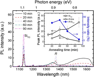
A quantitative correlation between R-line luminescence at around 1.37 µm and {311} defect nature, size and concentration has been undertaken in silicon, following keV Si-implantation and subsequent annealing using photoluminescence spectroscopy and plan-view transmission electron microscopy. The formation and evolution of the rod-like defects were found to be dependent on annealing time at a temperature of 700 °C, but there was no simple correlation found between the density and size of those defects and the R-line intensity. In particular, whereas the presence of {311} defects is essential for observing R-line luminescence, both very small {311} defects at short annealing times and fully developed {311} defects at long annealing times do not contribute to such luminescence. We provide possible explanations for this behavior and suggest that the local (strain) environment around defects, the dopant level and impurities in the silicon substrate may all play a role in determining R-line intensity.

Type
Research Letters
Copyright
Copyright © Materials Research Society 2012

Access options

Get access to the full version of this content by using one of the access options below. (Log in options will check for institutional or personal access. Content may require purchase if you do not have access.)

References

1.Chason, E., Picraux, S.T., Poate, J.M., Borland, J.O., Current, M.I., Diaz de la Rubia, T., Eaglesham, D.J., Holland, O.W., Law, M.E., Magee, C.W., Mayer, J.W., Melngailis, J., and Tasch, A.F.: Ion beams in silicon processing and characterization. J. Appl. Phys. 81, 6513 (1997).CrossRefGoogle Scholar
2.Libertino, S. and La Magna, A.: Damage formation and evolution in ion-implanted crystalline Si, in Materials Science with Ion Beams, Topics in Applied Physics Vol. 116, edited by Bernas, H. (Springer-Verlag, Berlin, 2010), pp. 147212.Google Scholar
3.Davies, G.: The optical properties of luminescence centres in silicon. Phys. Rep. 176, 83 (1989).CrossRefGoogle Scholar
4.Charnvanichborikarn, S.: Defect-Mediated Nanostructures and Luminescence Centres in Silicon. Ph.D. Thesis, The Australian National University (2011).Google Scholar
5.Davies, G., Lightowlers, E.C., and Ciechanowska, Z.E.: The 1018 meV (W or I1) vibronic band in silicon. J. Phys. C 20, 191 (1987).Google Scholar
6.Coomer, B.J., Goss, J.P., Jones, R., Öberg, S., and Briddon, P.R.: Interstitial aggregates and a new model for the I1/W optical centre in silicon. Physica B 273–274, 505 (1999).Google Scholar
7.Giri, P.K.: Photoluminescence signature of silicon interstitial cluster evolution from compact to extended structures in ion-implanted silicon. Semicond. Sci. Technol. 20, 638 (2005).Google Scholar
8.Schmidt, D.C., Svensson, B.G., Seibt, M., Jagadish, C., and Davies, G.: Photoluminescence, deep level transient spectroscopy and transmission electron microscopy measurements on MeV self-ion implanted and annealed n-type silicon. J. Appl. Phys. 88, 2309 (2000).CrossRefGoogle Scholar
9.Eaglesham, D.J., Stolk, P.A., Gossmann, H.-J., and Poate, J.M.: Implantation and transient B diffusion in Si: the source of the interstitials. Appl. Phys. Lett. 65, 2305 (1994).CrossRefGoogle Scholar
10.Yasutake, Y., Igarashi, J., Tana-ami, N., and Fukatsu, S.: An electric-field-active 1377-nm narrow-line Si light-emitting diode at 150 K. Opt. Express 17, 16739 (2009).CrossRefGoogle Scholar
11.Matthews, M.D. and Ashby, S.J.: The dynamic observation of the formation of defects in silicon under electron and proton irradiation. Philos. Mag. 27, 1313 (1973).Google Scholar
12.Coffa, S., Libertino, S., and Spinella, C.: Transition from small interstitial clusters to extended {311} defects in ion-implanted Si. Appl. Phys. Lett. 76, 321 (2000).Google Scholar
13.Giri, P.K., Coffa, S., and Rimini, E.: Evidence for small interstitial clusters as the origin of photoluminescence W band in ion-implanted silicon. Appl. Phys. Lett. 78, 291 (2001).Google Scholar
14.Davies, G., Harding, R., Jin, T., Mainwood, A., and Leung-Wong, J.: Optical studies of ion-implantation centres in silicon. Nucl. Instrum. Methods Phys. Res. B 186, 1 (2001).Google Scholar
15.Chou, C.T., Cockayne, D.J.H., Zou, J., Kringhøj, P., and Jagadish, C.: {111} defects in 1-MeV-silicon-ion-implanted silicon. Phys. Rev. B 52, 17223 (1995).Google Scholar
16.Lightowlers, E.C., Jeyanathan, L., Safonov, A.N., Higgs, V., and Davies, G.: Luminescence from rod-like defects and hydrogen related centres in silicon. Mater. Sci. Eng., B 24, 144 (1994).CrossRefGoogle Scholar
17.Biersack, J.P. and Haggmark, L.G.: A Monte Carlo computer program for the transport of energetic ions in amorphous targets. Nucl. Instrum. Methods 174, 257 (1980).Google Scholar
18.Wong-Leung, J., Fatima, S., Jagadish, C., Fitz Gerald, J.D., Chou, C.T., Zou, J., and Cockayne, D.J.H.: Transmission electron microscopy characterization of secondary defects created by MeV Si, Ge, and Sn implantation in silicon. J. Appl. Phys. 88, 1312 (2000).CrossRefGoogle Scholar
19.Libertino, S., Coffa, S., Spinella, C., La Magna, A., and Privitera, V.: Point defect diffusion and clustering in ion implanted c-Si. Nucl. Instrum. Methods Phys. Res. B 178, 25 (2001).Google Scholar
20.Cowern, N.E.B., Mannino, G., Stolk, P.A., Roozeboom, F., Huizing, H.G.A., van Berkum, J.G.M., Cristiano, F., Claverie, A., and Jaraíz, M.: Energetics of self-interstitial clusters in Si. Phys. Rev. Lett. 82, 4460 (1999).CrossRefGoogle Scholar
21.Weman, H., Monemar, B., Oehrlein, G.S., and Jeng, S.J.: Strain-induced quantum confinement of carriers due to extended defects in silicon. Phys. Rev. B 42, 3109 (1990).Google Scholar
22.Harding, R.E., Davies, G., Hayama, S., Coleman, P.G., Burrows, C.P., and Wong-Leung, J.: Photoluminescence response of ion-implanted silicon. Appl. Phys. Lett. 89, 181917 (2006).Google Scholar
23.Moller, K., Jones, K.S., and Law, M.E.: Cross-sectional transmission electron microscopy analysis of {311} defects from Si implantation into silicon. Appl. Phys. Lett. 72, 2547 (1998).Google Scholar
24.Stolk, P.A., Gossmann, H.-J., Eaglesham, D.J., Jacobson, D.C., Rafferty, C.S., Gilmer, G.H., Jaraíz, M., Poate, J.M., Luftman, H.S., and Haynes, T.E.: Physical mechanisms of transient enhanced dopant diffusion in ion-implanted silicon. J. Appl. Phys. 81, 6031 (1997).CrossRefGoogle Scholar
25.Pan, G.Z. and Tu, K.N.: Transmission electron microscopy on {113} rodlike defects and {111} dislocation loops in silicon-implanted silicon. J. Appl. Phys. 82, 601 (1997).Google Scholar
26.Takeda, S.: An atomic model of electron-irradiation-induced defects on {113} in Si. Jpn. J. Appl. Phys. 30, L639 (1991).Google Scholar
27.Haynes, T.E., Eaglesham, D.J., Stolk, P.A., Gossmann, H.-J., Jacobson, D.C., and Poate, J.M.: Interactions of ion-implantation-induced interstitials with boron at high concentrations in silicon. Appl. Phys. Lett. 69, 1376 (1996).Google Scholar
28.Brindos, R., Keys, P., Jones, K.S., and Law, M.E.: Effect of arsenic doping on {311} defect dissolution in silicon. Appl. Phys. Lett. 75, 229 (1999).CrossRefGoogle Scholar
29.Higgs, V., Lightowlers, E.C., Norman, C.E., and Kightley, P.: Characterisation of dislocations in the presence of transition metal contamination. Mater. Sci. Forum 83–87, 1309 (1992).Google Scholar
30.Tereshchenko, A.N., Steinman, E.A., and Mazilkin, A.A.: Effect of copper on dislocation luminescence centers in silicon. Phys. Solid State 53, 369 (2011).Google Scholar