Hostname: page-component-7c8c6479df-hgkh8 Total loading time: 0 Render date: 2024-03-19T08:48:03.267Z Has data issue: false hasContentIssue false

Detection of plasmonic behavior in colloidal indium tin oxide films by impedance spectroscopy

Published online by Cambridge University Press:  06 April 2020

Salil M. Joshi
Affiliation:
School of Materials Science and Engineering, Georgia Institute of Technology, Atlanta, GA30332, USA
Ning Xia
Affiliation:
School of Materials Science and Engineering, Georgia Institute of Technology, Atlanta, GA30332, USA
Yolande Berta
Affiliation:
School of Materials Science and Engineering, Georgia Institute of Technology, Atlanta, GA30332, USA
Yong Ding
Affiliation:
School of Materials Science and Engineering, Georgia Institute of Technology, Atlanta, GA30332, USA
Rosario A. Gerhardt*
Affiliation:
School of Materials Science and Engineering, Georgia Institute of Technology, Atlanta, GA30332, USA
Kenneth C. Littrell
Affiliation:
Neutron Scattering Division, Oak Ridge National Laboratory, Oak Ridge, TN37831, USA
Eric Woods
Affiliation:
The Institute for Electronics and Nanotechnology, Georgia Institute of Technology, Atlanta, GA30332, USA
Mengkun Tian
Affiliation:
The Institute for Electronics and Nanotechnology, Georgia Institute of Technology, Atlanta, GA30332, USA
*
Address all correspondence to Rosario A. Gerhardt at rosario.gerhardt@mse.gatech.edu
Get access

Abstract

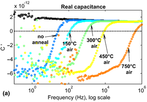
Impedance spectroscopy was conducted on colloidal ITO thin films that had been subjected to alternating oxygen and argon plasma treatments, followed by air annealing from 150 to 750 °C. An equivalent circuit consisting of an RC element nested within another RC element, featuring a negative resistance and a negative capacitance, fitted the data well. These results are interpreted as being due to surface plasmons that are a function of the presence of nanoporous ITO-rich regions surrounded by isolated ITO nanoparticles coated with an amorphous polymer that intertwines with the ITO-rich regions as a function of annealing treatment.

Type
Research Letters
Copyright
Copyright © Materials Research Society 2020

Access options

Get access to the full version of this content by using one of the access options below. (Log in options will check for institutional or personal access. Content may require purchase if you do not have access.)

References

1.Barsoukov, E. and Macdonald, J.R., eds: Impedance Spectroscopy: Theory, Experiment, and Applications. 2nd ed. (John Wiley & Sons, Hoboken, NJ, USA, 2005).CrossRefGoogle Scholar
2.Gerhardt, R.A.: Impedance spectroscopy and mobility spectra. In Encyclopedia of Condensed Matter Physics, Vol. 1, edited by Bassani, F., Liedl, G.L., and Wyder, P. (Elsevier Science, Amsterdam, 2005) pp. 350363.CrossRefGoogle Scholar
3.Macdonald, J.R.: Impedance spectroscopy. Ann. Biomed. Eng. 20, 289 (1992).CrossRefGoogle ScholarPubMed
4.Joshi, S.M., Book, G.W., and Gerhardt, R.A.: A comparative study of the effect of annealing and plasma treatments on the microstructure and properties of colloidal ITO films and cold-sputtered ITO films. Thin Solid Films 520, 2723 (2012).CrossRefGoogle Scholar
5.Wignall, G.D., Littrell, K.C., Heller, W.T., Melnichenko, Y.B., Bailey, K.M., Lynn, G.W., Myles, D.A., Urban, V.S., Buchanan, M.V., Selbye, D.L., and Butlerf, P.D.: The 40 m general purpose small-angle neutron scattering instrument at Oak Ridge National Laboratory. J. Appl. Cryst. 45, 8898 (2012).CrossRefGoogle Scholar
6.Pedersen, J.S.: Analysis of small-angle scattering data from colloids and polymer solutions: modeling and least-squares fitting I. Adv. Colloid Interface Sci. 70, 171 (1997).CrossRefGoogle Scholar
7.Joshi, S.M.: Effect of heat and plasma treatments on the electrical and optical properties of colloidal indium tin oxide films. Ph.D. Dissertation, Georgia Institute of Technology, Atlanta, GA, 2013.Google Scholar
9.Gerhardt, R.A.: Impedance and dielectric spectroscopy of nanoparticulate films and composites. In TechConnect Briefs, Volume 1: Nanotechnology 2013: Advanced Materials, CNTs, Particles, Films and Composites, Vol. 1. (2013) pp. 167170. https ://briefs.techconnect.org/papers/impedance-and-dielectric-spectroscopy-of-nanoparticulate-films-and-composites/ (ISBN: 978-1-4822-0581-7).Google Scholar
10.Cao, W., Gerhardt, R., and Wachtman, J.: Effect of sodium ions on the dielectric conductivity of porous silica in humid environments. MRS Proc. 195, 471 (1990).CrossRefGoogle Scholar
11.Gerhardt, R.A.: Impedance and dielectric spectroscopy revisited: distinguishing localized relaxation from long range conductivity. J. Phys. Chem. Solids 55, 1491 (1994).CrossRefGoogle Scholar
12.Muhlbauer, R.L., Joshi, S.M., and Gerhardt, R.A.: The effect of drying technique on the electrical properties of multiwalled carbon nanotube thin films deposited on paper substrates with different pore size. J. Mater. Res. 28, 1617 (2013).CrossRefGoogle Scholar
13.Khatami, Y., Kang, J., and Banerjee, K.: Graphene nanoribbon based negative resistance device for ultra-low voltage digital logic applications. Appl. Phys. Lett. 102, 043114 (2013).CrossRefGoogle Scholar
14.Kim, Y., Jang, J.H., Park, S.-J., Jesse, S., Donovan, L., Borisevich, A.Y., Lee, W., and Kalinin, S.V.: Local probing of electrochemically induced negative differential resistance in TiO2 memristive materials. Nanotechnology 24, 085702 (2013).CrossRefGoogle ScholarPubMed
15.Tzung-Min, T. and Yo-Sheng, L.: A 60-GHz double-balanced mixer with negative resistance compensation for direct up-conversion using 90-nm CMOS technology. Microw. Opt. Techn. Lett. 55, 536 (2013).Google Scholar
16.Bakueva, L., Konstantatos, G., Musikhin, S., Ruda, H.E., and Shik, A.: Negative capacitance in polymer-nanocrystal composites. Appl. Phys. Lett. 85, 3567 (2004).CrossRefGoogle Scholar
17.Chen, W.-C., Wen, T.-C., and Gopalan, A.: Negative capacitance for polyaniline: an analysis via electrochemical impedance spectroscopy. Synth. Met. 128, 179 (2002).CrossRefGoogle Scholar
18.Ehrenfreund, E., Lungenschmied, C., Dennler, G., Neugebauer, H., and Sariciftci, N.S.: Negative capacitance in organic semiconductor devices: Bipolar injection and charge recombination mechanism. Appl. Phys. Lett 91, 012112 (2007).CrossRefGoogle Scholar
19.El Kamel, F., Gonon, P., Jomni, F., and Yangui, B.: Observation of negative capacitances in metal-insulator-metal devices based on a-BaTiO3:H. Appl. Phys. Lett 93, 042904 (2008).CrossRefGoogle Scholar
20.Ershov, M., Liu, H.C., Li, L., Buchanan, M., Wasilewski, Z.R., and Jonscher, A.K.: Negative capacitance effect in semiconductor devices. IEEE Trans. Electron Dev. 45, 2196 (1998).CrossRefGoogle Scholar
21.Ke, Q., Lou, X., Yang, H., Kumar, A., Zeng, K., and Wang, J.: Negative capacitance induced by redistribution of oxygen vacancies in the fatigued BiFeO3-based thin film. Appl. Phys. Lett. 101, 022904 (2012).CrossRefGoogle Scholar
22.Wu, X., Yang, E.S., and Evans, H.L.: Negative capacitance at metal-semiconductor interfaces. J. Appl. Phys. 68, 2845 (1990).CrossRefGoogle Scholar
23.Bertram, B.D. and Gerhardt, R.A.: Room temperature properties of electrical contacts to alumina composites containing silicon carbide whiskers. J. Appl. Phys. 105, 074902 (2009).CrossRefGoogle Scholar
24.Parravicini, G.B., Stella, A., Ungureanu, M.C., and Kofman, R.: Low-frequency negative capacitance effect in systems of metallic nanoparticles embedded in dielectric matrix. Appl. Phys. Lett. 85, 302 (2004).CrossRefGoogle Scholar
25.van Zyl, R., Perold, W., and Botha, R.: The Gunn-diode: Fundamentals and fabrication. IEEE Proceedings of 1998 South African Symposium on Communications and Signal Processing, Rondebosch, South Africa, 1998; p. 407.Google Scholar
26.Alekseev, E., Pavlidis, D., Sutton, W.E., Piner, E.L., and Redwing, J.: GaN-based Gunn diodes: Their frequency and power performance and experimental considerations. IEICE Trans. Electron E84C, 1462 (2001).Google Scholar
27.Forster, A., Lepsa, M.I., Freundt, D., Stock, J., and Montanari, S.: Hot electron injector Gunn diode for advanced driver assistance systems. Appl. Phys. A 87, 545 (2007).CrossRefGoogle Scholar
28.Jonscher, A.K.: The physical origin of negative capacitance. J. Chem. Soc. Faraday Trans. 82, 75 (1986).CrossRefGoogle Scholar
29.Granqvist, C.G. and Hultåker, A.: Transparent and conducting ITO films: new developments and applications. Thin Solid Films 411, 1 (2002).CrossRefGoogle Scholar
Supplementary material: PDF

Joshi et al. Supplementary Materials

Joshi et al. Supplementary Materials

Download Joshi et al. Supplementary Materials(PDF)
PDF 1.4 MB