


Introduction
Materials research provides the foundation for the development of many new technologies. Basic materials research in the United States is supported by several federal agencies, including the National Science Foundation (NSF), Department of Energy (DOE), and Department of Defense (DoD). Federal agencies play a critical role not only in funding research at universities and national laboratories, but also in forging collaborations with industrial partners. At NSF, the Division of Materials Research (DMR), in particular, is dedicated to advancing fundamental materials research through single investigator grants, as well as through research centers, such as the Materials Research Science and Engineering Centers. To help identify and highlight important emerging areas of materials research, funding agencies often solicit input from the community by holding workshops and conducting outreach at meetings run by the Materials Research Society (MRS) and other professional societies.
The Electronic and Photonic Materials (EPM) Program within NSF DMR sponsored a workshop titled “Current Challenges and Future Opportunities in Electronic and Photonic Materials” on September 25–26, 2017. The goals of the workshop were threefold: (1) to better understand what the community views as current frontiers and future opportunities for electronic and photonic materials research, (2) to assess the community’s readiness to address important national issues and societal needs, and (3) to identify gaps and new areas for EPM research in the near future. The range of materials within the scope of the EPM program is very broad. To allow more in-depth discussions, the workshop focused on four classes of materials: epitaxially grown materials (semiconductors, oxides, and hybrid materials); van der Waals (vdW) materials; organic/flexible materials; and metamaterials. Approximately 30 invited participants attended this workshop and contributed to a written report, which can be found at https://sites.cns.utexas.edu/epm_nsf_workshop.
This article reports on the outcomes of the workshop and provides a framework for describing EPM research. It reflects the opinions of the authors and not those of the NSF. We first summarize the authors’ perceptions of major drivers of EPM research and a means of characterizing the scope of activity. We then summarize the workshop discussions of recent breakthroughs, outstanding challenges, possible approaches to address these challenges, and future opportunities associated with the four classes of materials. We conclude by identifying the broader impacts of EPM research, including potential contributions to national initiatives. We aim to provide new students and postdoctoral researchers with a framework to identify opportunities to participate in EPM research and to define important frontiers for all interested investigators.
Scope of EPM research
The search for new properties and application paradigms is a major driver of materials research. EPM research encompasses a broad range of activities, from the discovery of new properties and phenomena, to the exploration of applications. The motivation for an EPM research program can be framed by defining targets that prescribe a set of aligned activities (Figure 1). For example, the advantages of new computing paradigms that manipulate information stored in quantum states drive research on quantum materials with appropriately coupled or decoupled degrees of freedom. Novel properties may arise in classes of materials with distinctive features in their band structure, as in topological materials. Research may also target understanding of tailored interactions at microscopic and mesoscopic length scales that lead to new phenomena, such as in metamaterials. Many important frontiers in materials research can be identified in this manner, including electronic phases of matter, the coexistence of phases such as ferromagnetism and superconductivity, and metamaterials with tunable responses. Understanding the coupled degrees of freedom enables a quantitative description of the material response to an external perturbation, particularly electromagnetic fields, photons, and heating.
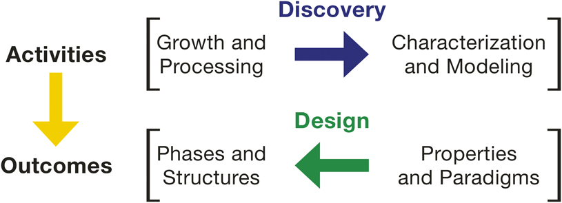
Figure 1. Taxonomy for electronic and photonic materials research.
To guide research, particularly on more mature classes of materials, it is helpful to identify target material phases and structures that exhibit the properties and phenomena of interest in a specified application space. Semiconducting and dielectric materials are typically further classified in terms of their composition (e.g., III–V, transition-metal oxides, transition-metal dichalcogenides) and band structure (e.g., direct, indirect, intermediate). Going beyond the specification of bulk phases, the mesoscale structure can also be a useful descriptor for many active areas of EPM research. “Low dimensional” materials, including quantum dots, nanowires, and quantum wells, offer dimensionality as a means to engineer useful properties. For these less mature materials, the expectation of emergent properties may itself be the motivation for research.
By extension, heterostructures and assemblies may be targeted to produce novel combinations of properties not present in single-phase materials, either in an additive fashion or through their interactions. The frontiers in targets defined by phases and structures include ordered composites that function as metamaterials, multiphase materials such as bulk heterojunctions, complex ternary and quaternary compounds, and mixed-dimensional heterostructures. We also note that the potential advantages of printing materials (electronic and photonic) rapidly over large areas can be used to motivate target properties or routes to processing.
A large toolbox of growth and processing methods is necessary to achieve diverse target phases and structures. Thin-film growth techniques, including atomic layer deposition, chemical vapor deposition, and molecular beam epitaxy, are well represented in EPM research. Epitaxial thin films are typically grown on single-crystal substrates cut from bulk crystals; important targets of understanding include the influence of defects and strain on nucleation and growth, and epitaxy in the presence of weak van der Waals interactions. Such understanding is important insofar as it is enabling of the growth of structures with distinct or superior properties. Organic materials and many low-dimensional materials mentioned previously can be synthesized via solution-based processes in addition to vapor-phase deposition. Solution processing is of interest because it can facilitate large-scale synthesis, large-scale printing, nanopatterning, and self-assembly. Frontiers in materials growth and processing include the engineering of defects and strain; selected area growth and etching; controlling nanoscale structure and composition of freestanding structures and heterostructures; and heterogeneous integration by direct growth.
Theory, characterization, and modeling elucidate the structure–property relationships that define the knowledge goals of EPM research. These provide an understanding of processes during growth, the degree to which target structures have been achieved, and the properties of phases, nanostructures, and heterostructures (i.e., their response to perturbations). For targets including phases and structures, the characterization of microstructure and composition via microscopy and spectroscopy is of central importance. Spectroscopies and transport measurements enable the analysis of ground- and excited-state electronic, optical, thermal, and magnetic properties. The frontiers of characterization are advanced through improvements in spatial, temporal, and energy resolution, and through methods of correlating characterization methods. Theory, modeling, and computation provide both a necessary framework for interpreting the output of characterization efforts and a means to identify promising new avenues to explore. Opportunities to advance the frontiers of EPM research arise from the greater integration of experimental work, both benchtop and in simulations, with theory and modeling in complementary and synergistic ways. The monitoring of growth processes in situ and materials in devices in operando is another important frontier.
When key structure–property relationships have been established, advances can be driven by the application of design principles. Heteroepitaxy provides a route to control strain in thin films, which enables the design of properties via strain engineering. The development of photonic crystals based on the understanding of electronic band structure is an example of material evolution driven by design.Plasmonic structures and metamaterials are composite materials whose structure can be designed to achieve target properties. At the frontiers of these fields, performance becomes limited by the ability to pattern nanostructures or the perfection of materials structures and interfaces. These limits may drive additional research in the growth and processing of single-phase materials.
Not all materials research proceeds from desired properties to proposed structures; many advances in EPM arise from the pursuit or discovery of new structures in which novel properties emerge and, subsequently, motivate application-inspired basic research. The discovery of carbon nanotubes led to an explosion of research in synthesis, characterization of structure and properties, and the exploration of very diverse applications. A similar evolution is occurring in the fields of colloidal semiconductor nanocrystals, semiconductor nanowires, and more recently in two-dimensional (2D) or vdW materials. Colloidal nanocrystals acting as zero-dimensional (0D) quantum dots are now incorporated in commercial display technologies, whereas applications for 2D materials are still emerging. Interestingly, the authors have observed similar trends in MRS symposia, which reveal a consistent pattern of evolution in materials research categorized by reduced dimensionality (e.g., 0D, 1D, or 2D). Rapidly increasing attention to a particular class of materials leads to large symposia covering the full scope of research from basic synthesis to proof-of-principle applications. As the field matures and more investigators enter, more symposia are organized around particular applications (e.g., “low-dimensional materials for solar water splitting”). These cycles can be very short when many researchers are well poised to apply well-developed methods to new materials, as in the case of hybrid perovskites. Because the community organizes MRS symposia in a bottom-up fashion, they reflect the diverse ways that EPM research can be classified and pursued.
The NSF EPM workshop, summarized in this article, was organized around working groups representing several active areas of EPM research, including Epitaxial Materials, van der Waals Materials, Organic and Flexible Materials, and Metamaterials (see Figure 2).Reference Yu, Genevet, Kats, Aieta, Tetienne, Capasso and Gaburro1–Reference Venkateshvaran, Nikolka, Sadhanala, Lemaur, Zelazny, Kepa, Hurhangee, Kronemeijer, Pecunia, Nasrallah, Romanov, Broch, McCulloch, Emin, Olivier, Cornil, Beljonne and Sirringhaus4 Each represents a different approach to classifying EPM research, as discussed previously. The term “Epitaxial Materials” refers explicitly to an activity or approach, but more broadly to opportunities to engineer properties through strain engineering and the potential for impacting associated with growing materials on established platform substrates, such as Si. “Van der Waals Materials” refers to the structure, specifically the interlayer vdW bonds in layered materials, but encompasses a vast range of materials properties that might be combined by new material fabrication routes. “Organic and Flexible Materials” references both composition and a desirable performance attribute that is present in other classes of materials, but organics are relatively advanced in their application to displays and thin-film transistors. “Metamaterials” may be broadly defined as hierarchically structured materials with properties not found in single-phase materials. The term is most often applied to materials with artificially engineered electromagnetic responses, and thus metamaterials are represented within the EPM portfolio. There are other ways to classify EPM research, not captured by these topics.
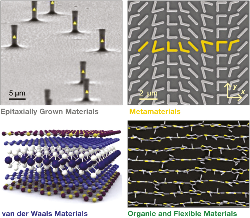
Figure 2. Four classes of materials discussed at the Electronic and Photonic Materials Program workshop.Reference Yu, Genevet, Kats, Aieta, Tetienne, Capasso and Gaburro1–Reference Venkateshvaran, Nikolka, Sadhanala, Lemaur, Zelazny, Kepa, Hurhangee, Kronemeijer, Pecunia, Nasrallah, Romanov, Broch, McCulloch, Emin, Olivier, Cornil, Beljonne and Sirringhaus4
Challenges and opportunities
Epitaxial materials
Epitaxial crystal growth started a revolution some 50 years ago by enabling thin-film compounds and semiconductor devices that have led to many fundamental scientific discoveries. Epitaxial materials also form the foundation for a wide range of technologies, including smart lighting, self-driving cars, fiber-optic communication, medical diagnostics, and mobile devices. The power and promise of epitaxial materials lie in atomic-control in all dimensions to design materials and artificial structures. Epitaxially grown materials also offer a route to integrating materials with complementary functionality and for scale-up integration in devices. Research continues to push the frontiers to achieve more precise atomic-scale control with in situ feedback, manipulations of substrate properties, combinations of dissimilar materials, and complex modeling of growth mechanisms.
Current epitaxial materials research takes commercial technologies, such as molecular beam epitaxy and organometallic vapor-phase epitaxy, and applies them in new ways to fabricate structures. Because of the diversity of epitaxial materials, the NSF-EPM report addressed several representative classes of materials, including III–V nanowires, III–V quantum dots (Figure 3a),Reference Tatebayashi, Kako, Ho, Ota, Iwamoto and Arakawa5 Group III nitrides (Figure 3b), Group III antimony, epitaxial spintronic materials (Figure 3c),Reference Brown-Heft, Logan, McFadden, Guillemard, Le Fèvre, Bertran, Andrieu and Palmstrøm6 and epitaxial oxides (Figure 3d).Reference Fredrickson, Ponath, Posadas, McCartney, Aoki, Smith and Demkov7 Van der Waals epitaxy was also discussed in the vdW materials section.
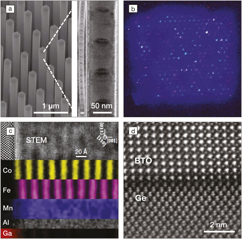
Figure 3. Images of representative epitaxial materials. (a) Scanning electron microscope image of GaAs/AlGaAs/GaAs nanowires and STEM image of stacked InGaAs/GaAs quantum dots embedded inside the nanowires.Reference Tatebayashi, Kako, Ho, Ota, Iwamoto and Arakawa5 (b) Array of GaN nanowire (400 nanowires from left to right) light-emitting diodes. Figure courtesy of M.D. Brubaker and K.A. Bertness, NIST. (c) STEM image of CoMnAl and FeMnAl superlattices grown on a GaAs substrate.Reference Brown-Heft, Logan, McFadden, Guillemard, Le Fèvre, Bertran, Andrieu and Palmstrøm6 (d) Transmission electron microscope image of a BaTiO3 (BTO) film grown on a Ge substrate.Reference Fredrickson, Ponath, Posadas, McCartney, Aoki, Smith and Demkov7
Some challenges facing epitaxial growth are materials-specific (e.g., how to increase breakdown voltage and p-doping for Group III nitride growth, how to increase the growth rate for oxides, and how to control the three-dimensional (3D) growth of semiconductor nano-wires). Other challenges are general, including how to control quaternary alloy growth and how to model atomic surface diffusion including strain energy minimization and the corresponding metrology to guide theory. Another common challenge facing epitaxial materials growth is to understand and control the interface because device functionality is often derived from the interface. Understanding the chemistry and bonding at the interface, developing new strategies for surface passivation, and controlling defect types and density are all critical issues; characterization methods capable of monitoring materials composition and phase stability at the atomic and nanoscale, therefore, can have a tremendous impact.
Choosing and developing proper substrates have always been important considerations and challenges in epitaxial materials. More recently, “dissimilar materials epitaxy” has been adopted as a strategy to combine different materials for expanded and integrated functionalities. Notable examples include the growth of ferromagnetic metals on semiconductors, superconductors on semiconductor nanowires for exploring the formation of Majorana fermions, and III-Sb and transition-metal oxides on foreign substrates (e.g., GaAs, Si, and Ge). Understanding the thermodynamics and consequences of different crystal symmetries and atomic bonding at the interfaces between dissimilar materials will help minimize the impact of inherent defects on device performance.
Epitaxial materials will continue to have a significant impact on both fundamental science and technologies. Areas that are particularly ripe for expansion in the next decade are topological materials, quantum information and quantum optics, neuromorphic devices, and micro- and nanoscale integration of multiple electromagnetic functions. To pursue these opportunities, scientific challenges, as well as those of an institutional nature, must be solved. In particular, there is a critical need for stable infrastructure support as epitaxy tools and related characterization equipment require not only periodic capital funding but maintenance funding as well.
Van der Waals materials
The atoms within a 2D layer in vdW materials are connected by covalent or ionic bonds, whereas the layers are held together via weak vdW interactions. Because of the weakness of vdW forces, monolayers or few-layers-thick materials can be created using a variety of growth techniques. Tremendous opportunities exist to exploit tunable coupling between monolayers as a new paradigm to manipulate different degrees of freedom, such as the spin and valley degree of freedom. Recent research has increasingly shifted toward heterostructures, formed by assembling or directly growing atomically thin layers either laterally or vertically (Figure 4a). These heterostructures feature the combined functionality of the individual layers and may even lead to emergent properties.
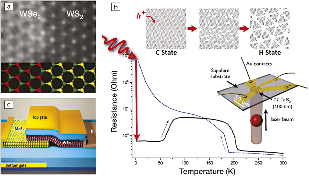
Figure 4. (a) Transmission electron microscope image of a lateral heterostructure consisting of WSe2 and WS2 monolayers.Reference Zhang, Chen, Duan, Zang, Luo and Duan8 (b) Insulator-to-metal transition in TaS2 under light illumination associated with charge density waves.Reference Stojchevska, Vaskivskyi, Mertelj, Kusar, Svetin, Brazovskii and Mihailovic9 (c) Illustration of a tunnel diode consisting of vertically stacked few-layer-thick WSe2 and MoS2.Reference Roy, Tosun, Cao, Fang, Lien, Zhao, Chen, Chueh, Guo and Javey10
The discussions at the workshop focused on three scientific themes: (1) new concepts for electronic and optoelectronic devices based on couplings between internal degrees of freedom, such as “valleytronics”; (2) new electronic phases and new devices arising from strong coupling to external fields in ultrathin vdW materials; and (3) new behaviors arising from coupling between vdW layers in “stacked” heterostructures.
The growth and processing of vdW materials are key enablers of scientific discovery and potential new technology. Although a significant number of novel electronic and optical devices have been demonstrated through the use of 2D materials obtained by exfoliation and transfer, far fewer such devices have been fabricated using materials produced by epitaxial growth, which is a critical step toward providing a scalable platform. With the continued development of such growth methods for 2D materials,Reference Zhang, Chen, Duan, Zang, Luo and Duan8 there is a great opportunity to impact the field of wafer-scale novel electronic and photonic devices.
Characterization of 2D crystals and their heterostructures has been performed with a range of experimental techniques covering atomic to macroscopic length scales. The most fruitful scientific outcomes result from a collaborative approach involving theoretical calculations and multi-length-scale experimental probes on the highest quality materials. Electron microscopy and several forms of scanning probe microscopy have been utilized to characterize both atomic and electronic structure at microscopic length scales. Optical studies, such as photoluminescence and Raman spectroscopy, have been essential in exploring structures and electronic excitations and degrees of freedom. However, simple linear optical spectroscopy methods do not reveal dynamic information and are limited in spatial resolution by diffraction. There is a critical need to develop methods to characterize the optical properties of 2D crystals and their heterostructures to the deep sub-diffraction length scale (<<100 nm) and on ultrafast time scales. In addition, there is still a knowledge gap between real-space and k-space investigations of the electronic structures of such materials at the nanoscale. To this end, the development of nanoscale k-space probes of electronic structure, such as nanoscale angle-resolved photoemission spectroscopy, is of high interest.
The study of novel phases arising from many-body interactions and cooperative couplings between different fundamental degrees of freedom is of great significance for electronic materials and has produced several recent breakthroughs in vdW materials. There are many challenges to exploring new phases in 2D materials, including the growth and assembly of high-quality vdW layers and heterostructures, understanding the role of defects, disentangling and modeling the complex physics of cooperative quantum phasesReference Stojchevska, Vaskivskyi, Mertelj, Kusar, Svetin, Brazovskii and Mihailovic9 (Figure 4b), and further developing and applying advanced characterization techniques.
VdW materials offer a rich platform to explore fundamental science with many recent breakthroughs. Their impact on studies of quantum materials and promise in quantum information technologies are widely recognized by the scientific community. While a large number of prototypical electronic and photonic devicesReference Roy, Tosun, Cao, Fang, Lien, Zhao, Chen, Chueh, Guo and Javey10 have been demonstrated in research laboratories (Figure 4c), it remains challenging to identify the most compelling applications to pursue. To translate vdW materials into industrial applications, large-scale synthesis, and assembly techniques, an improved understanding of defects, performance benchmarking, and new computational methods all need to be developed.
Organic and flexible materials
Flexible and/or organic electronic and photonic technology platforms could have a wide-ranging impact on daily life—especially when traditional limitations of their inorganic counterparts, generally imposed by size, weight, and compatibility, can be overcome. Organic materials and devices are shaping the field of electronics. Nowhere is this more apparent than in the mobile electronics market where organic light-emitting diodes are fast becoming the dominant display technology.
Generally, organic and flexible electronics materials have been envisioned to enable a broad range of versatile platforms. In addition to more established displays and lighting applications, other emerging electronic and photonic components include printed radio-frequency identification tags and memories; wearable or “imperceptible” electronics; ultrahigh mobility transistors that allow new, low-cost, large-area computation technology; electronically pumped lasers; building-integrated photovoltaics and off-grid solar panels; smart packaging products (e.g., for sensitive products such as food and drugs); smart labels for counterfeit protection or logistics purposes; and compact and skin-compatible analytical systems (Figure 5) that enable continuous monitoring for medical diagnostics or environmental analysis, to name a few examples.
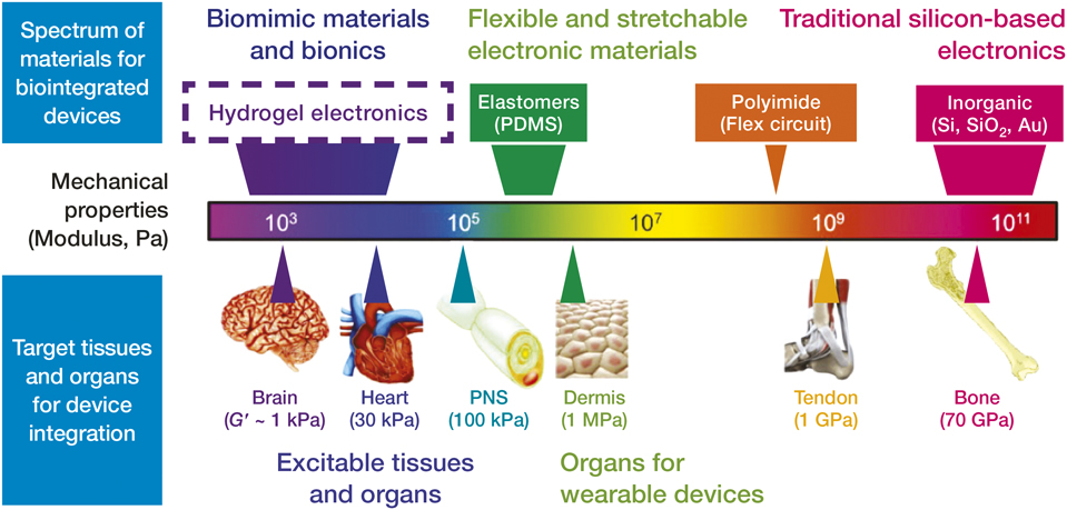
Figure 5. The properties of organic and flexible electronic materials can be readily directed via fine-tuning of chemical structure and molecular assembly. This is required, for instance, to harmonize mechanical properties for applications in the biointegrated electronics/bioelectronics area, leading to opportunities to engineer elastomeric and hydrogel-based electronic materials for applications in wearable and implantable devices, respectively. PDMS, poly(dimethylsiloxane); PNS, peripheral nervous system.
Possible applications for such components are wide-ranging; their use in an autonomous intelligent environment by the “Internet of Things”—human/machine interfaces, electronic skins, wearable electronics, and beyond—can be readily envisioned. This ambition to define future technologies has been fueled by the development of a plethora of new materials and materials platforms that have allowed the broad field of organic and flexible electronics to produce scientific and technological progress—in the United States and worldwide.
Organic and flexible materials platforms are also of fundamental interest. Complex photophysical processes occur in these multifaceted materials systems (charge-generation/recombination, light emission, polaron coherence, hybrid excitons and polaritons), and they may sustain multiple charge-transport mechanisms (electronic-, ionic-, mixed conduction). Processing and other environmental conditions can be used to fine-tune and optimize overall properties and device function (e.g., through the use of nucleating agents, annealing procedures, or exposure to aqueous environments with high ionic strengths). Yet, because of this versatility and breadth, realizing step changes can be challenging and often requires approaches across the entire materials chain: from materials design and synthesis; materials characterization; with the correlation of processing, structure, and properties; materials theory; and modeling, device fabrication, and characterization, to prototype manufacturing and product development. It also renders the establishment of a deep understanding of these materials systems an intricate task. Pronounced knowledge gaps still stifle progress in the area of organic and flexible electronics. There is still some way to go before the full potential of organic and flexible electronic materials systems is widely exploited.
What is clear is that the organic and flexible materials platform offers exciting and fascinating opportunities in a wide variety of areas, from energy harvesting and storage, to sustainable living and green cities, and health care. In addition, new possibilities continuously arise. For instance, alternative materials systems are advanced and/or rediscovered, from solution-processable quantum dots or metal-halide perovskite systems to 2D materials. Many of these are poised to assume a critical role in the development of future flexible technologies, for example, new quantum information technology based on the formation and detection of “entangled photons.” The ability to easily modify these material classes via changes in molecular chemistry; in a seemingly infinite variety of ways, provides a unique opportunity to exploit organics and other flexible materials for new applications that are inaccessible to conventional semiconductors to gain the ability to engineer “materials on demand” for a virtually endless range of purposes.
Metamaterials
The broad field of metamaterials is aimed at designing and synthesizing artificial materials with exotic properties, which do not exist in naturally occurring materials, by combining new materials science developments with sophisticated photonic engineering in subwavelength artificial unit cells or inclusions. A few examples of recent representative metamaterials are shown in Figure 6. The most distinctive feature of metamaterials is that their properties emerge at the mesoscale from the arrangement, shape, design, and composition of the basic unit cells of which they are formed, rather than from the molecular or atomic constituents, as in conventional materials. This field has been driven in the last two decades by the rapid development in computational power, new physical concepts, materials development, nanofabrication techniques, and characterization tools.
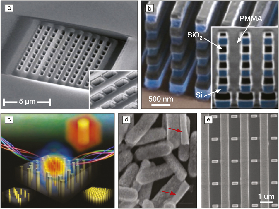
Figure 6. (a) Scanning electron microscope (SEM) image of a 3D negative refractive-index material.Reference Yang, Wang, Moitra, Kravchenko, Briggs and Valentine14 (b) SEM image of a 3D near-zero index metamaterial.Reference Moitra, Yang, Anderson, Kravchenko, Briggs and Valentine15 (c) Schematic of a self-assembled nanorod metamaterial.Reference Li, Sun, Gomez-Diaz, Hogan, Lu, Khatkhatay, Zhang, Jian, Huang, Su, Fan, Jacob, Li, Zhang, Jia, Sheldon, Alù, Li and Wang11 (d) Magnetically switchable self-assembled metamaterial.Reference Greybush, Saboktakin, Ye, Della Giovampaola, Oh, Berry, Engheta, Murray and Kagan12 (e) Broadband, ultrathin self-assembled polarizing metasurface.Reference Chen, Tymchenko, Gopalan, Ye, Wu, Zhang, Murray, Alu and Kagan13 Note: PMMA, poly(methyl methacrylate).
While early accomplishments in this field were motivated by the simple goal of engineering the effective constitutive parameters (e.g., permittivity and permeability) of bulk metamaterials, the most recent breakthroughs have been made possible via diverse approaches. Examples include the suitable combination of different phenomena over a unified materials platform (e.g., via quantum optical, optomechanical, and acousto-electrical phenomena), developing new self-assembly approaches (Figure 6c–e),Reference Li, Sun, Gomez-Diaz, Hogan, Lu, Khatkhatay, Zhang, Jian, Huang, Su, Fan, Jacob, Li, Zhang, Jia, Sheldon, Alù, Li and Wang11–Reference Chen, Tymchenko, Gopalan, Ye, Wu, Zhang, Murray, Alu and Kagan13 expanding the frequency range of operations (e.g., ultraviolet and near- to mid-infrared), integrating metamaterial designs with quantum materials and achieving extreme materials parameters (e.g., index near zero and large nonlinear susceptibility as in Figure 6a–b).Reference Yang, Wang, Moitra, Kravchenko, Briggs and Valentine14,Reference Moitra, Yang, Anderson, Kravchenko, Briggs and Valentine15
The key challenges that have prevented a broader range of applications of metamaterials can be summarized as limitations in loss, scale, scalability, and bandwidth. The loss of noble metals in the visible spectrum or of oxides in the near- to mid-infrared is too large to realize metamaterials with functionalities that can outperform natural materials for practical applications. In addition, the requirement of subwavelength inclusions makes fabrication of metamaterials operating in the short wavelength range challenging. In this context, fabrication methods can be divided into “top-down” and “bottom-up” approaches. While top-down approaches based on advanced tools such as e-beam lithography provide excellent control of ∼50 nm or larger dimensions, these fabrication methods are not only expensive and time-consuming, but also face serious challenges in reaching smaller length scales or in realizing 3D structures. As an alternative approach, direct laser writing, can produce 3D structures, but only with dimensions comparable to the laser wavelength, which fundamentally limits the range of frequencies over which this technique can be applied to metamaterials. In addition, many metamaterial designs are limited to a narrow spectral range even in ideal situations, because of constraints associated with passivity and causality, which further hinder the broad applicability of these materials in practical devices.
Much of the promise of metamaterials can be fulfilled by further reducing the dimensions of the artificial unit cells and by developing scalable synthesis methods. Self-assembly offers clear advantages in both aspects. Small unit cells with dimensions of ∼3–5 nm can be produced rapidly and in large quantities (Figure 6c–e). Nanocrystal assembly is typically driven by entropy and yields a close-packed arrangement. Development of synthesis methods producing open and arbitrary architectures will allow for many new possibilities. Gain and nonlinearities open other exciting opportunities in this context to break the limits of causality and passivity. Simulations and theory capable of incorporating quantum properties and active inclusions are necessary to accelerate the leap in metamaterial technology.
Producing an array of structures with uniform or controlled shape, size, and composition has been a common goal of materials synthesis in general. Such well-controlled artificial unit cells can be used as building blocks of metamaterials. So far, many metamaterial designs operate on enhanced light–matter interactions made possible by plasmonic resonances. By expanding such design principles and by utilizing a broader range of materials, new functionalities may be realized.
Several research areas have been identified as particularly promising for future exploration. Experimental realizations of multilayer- or multicomponent metamaterials will bring many opportunities. Dynamically reconfigurable metamaterials based on phase-change materials, liquid crystals, carrier injection, mechanical actuation, and nonlinearity will drastically expand the operation bandwidth. Both spatial and temporal modulations of materials properties introduce new unique properties. Increasing the depth or contrast of modulations can be a key enabling element for breakthroughs in metamaterials. Analogies between electronics, condensed-matter physics, and photonics have led to various new concepts, including optical metatronics, parity-time symmetry, and topological photonics. Metamaterials offer a unique platform for realizing these concepts. Low energy information processing based on metamaterials points to a new route for parallel processing when integrated with traditional information processing devices.
Cross-cutting trends
Some common challenges exist in developing different classes of materials, including the need for implementing in situ characterization tools, better control over interfacial properties, and more efficient computational methods to discover new materials. Common goals include establishing structure–property correlations, realizing scalable synthetic routes, and understanding the interactions and strong correlations between different phases. The toolsets available to the community are rapidly expanding. Improving access to these tools and cultivating effective collaborations across different sectors of the research community will catalyze breakthroughs. Exciting advances in big data, machine learning, and artificial intelligence have the potential to accelerate progress in materials research as explored in recent MRS symposia.
Outcomes and broader impacts
Research activities supported by the NSF-EPM programs are essential for enabling both new scientific discoveries and transformative engineering solutions to electronic and photonic industries. Training young researchers and increasing the number of participants from underrepresented groups in the science, technology, engineering, and mathematics fields are equally valued priorities for NSF-funded programs. The broader impacts of NSF-funded projects are realized in naturally integrated research and education programs.
Because of its unique role in bridging basic fundamental science and engineering, research supported by NSF-EPM is interdisciplinary and serves to connect different funding agencies and national initiatives. For example, the Materials Genome Initiative may accelerate material discovery via collaborative efforts between computation, synthesis, and characterization. All materials classes discussed at the workshop can support the realization of a “quantum leap” by developing materials platforms for emergent correlated phases, new topological orders, single photon emitters, entangle photon sources, or photonic structures for quantum interconnects. Some outcomes of EMP-supported research, such as biointegrated electronics based on flexible and organic materials, can contribute to the “Brain Initiative” by “advancing innovative neurotechnology.” Likewise, Brain Initiative-led discoveries (e.g., brain-like computing) may apply to accelerate material discovery.
Collaboration between academic institutions and national laboratories has always been fruitful and mutually beneficial. Nanoscale Science Research Centers, supported by the DOE, and neutron scattering facilities, supported by the DOE and the National Institute of Standards and Technology (NIST), are exemplary efforts along this direction. The impact of EPM research will be expanded via close collaborations with industrial partners. One outstanding example is the Semiconductor Research Corporation, which has provided a successful platform for public–private research collaborations for 35 years. Driven by the challenges at the end of complementary metal oxide semiconductor scaling, industry is eager to explore basic research of novel materials. The timing is ripe to expand such partnerships and collaborations.
Acknowledgments
The workshop and collaborative work in generating the report and this article are supported by NSF DMR-1748163. The contribution of Kris Bertness at NIST is gratefully acknowledged.


