


Introduction
The field of atomic-scale energy-dispersive X-ray (EDX) mapping is rapidly expanding. This is largely due to the development of silicon drift detectors (Lechner et al., Reference Lechner, Fiorini, Hartmann, Kemmer, Krause, Leutenegger, Longoni, Soltau, Stotter, Stotter, Struder and Weber2001; Phillips et al., Reference Phillips, Paulauskas, Rowlands, Nicholls, Low, Bhadare and Klie2014) with a larger solid angle and, therefore, higher detection rates. In addition, aberration correction (Watanabe et al., Reference Watanabe, Ackland, Burrows, Kiely, Williams, Krivanek, Dellby, Murfitt and Szilagyi2006) allows more electron current to be focused into an Angstrom-sized spot, increasing the rate of X-ray generation from a single atomic column. The result is a significant improvement in the final number of detected X-ray counts, so that atomic-scale EDX mapping (Allen et al., Reference Allen, D'Alfonso, Freitag and Klenov2012; Kotula et al., Reference Kotula, Klenov and Von Harrach2012; Itakura et al., Reference Itakura, Watanabe, Nishida, Daio and Matsumura2013; Chen et al., Reference Chen, Weyland, Sang, Xu, Dycus, LeBeau, D'Alfonso, Allen and Findlay2016; Lu et al., Reference Lu, Moya, Yuan and Zuo2018; Yang et al., Reference Yang, Quy Tran, Yamamoto, Yoshioka, Somidin, Nogita and Matsumura2020) is now possible for reasonable acquisition times of under an hour per map on beam-resilient samples. The improvement in raw X-ray counts is especially important for EDX quantification, as the limiting error in transmission electron microscopy (TEM) analysis has typically been poor counting statistics.
When the incident beam direction is aligned along a low-order zone axis of a crystalline material, as is necessary for atomic-resolution characterization, the aligned columns of atoms behave similarly to miniature lenses (Cowley et al., Reference Cowley, Spence and Smirnov1997; van den Bos et al., Reference van den Bos, De Backer, Martinez, Winckelmans, Bals, Nellist and Van Aert2016), providing a focusing effect on the beam. The resulting strong concentration of the beam to the atomic columns enhances the signal—which could be ADF (annular dark-field), EDX, or EELS (electron energy loss spectroscopy)—at atomic column sites, resulting in significant improvements in peak-to-background contrast. Electron channeling is often beneficial, as it improves the contrast in atomic-scale images (Lu et al., Reference Lu, Xiong, Van Benthem and Jia2013, Reference Lu, Moya, Yuan and Zuo2018) and can more than double the X-ray signal (relative to when channeling does not occur) (MacArthur et al., Reference MacArthur, Brown, Findlay and Allen2017). However, while this helps produce more aesthetically pleasing images, it also results in X-ray spectra where intensities can no longer be interpreted as comprising linear contributions from each element within the system (Lugg et al., Reference Lugg, Kothleitner, Shibata and Ikuhara2015; MacArthur et al., Reference MacArthur, Brown, Findlay and Allen2017). This is problematic, because the assumption that the X-ray signal is linearly proportional to the mass of the sample being illuminated by the beam is the basis for all EDX quantification methods: k-factors (Cliff & Lorimer, Reference Cliff and Lorimer1975), zeta-factors (Watanabe et al., Reference Watanabe, Horita and Nemoto1996; Watanabe & Williams, Reference Watanabe and Williams2006), and cross-sections (MacArthur et al., Reference MacArthur, Slater, Haigh, Ozkaya, Nellist and Lozano-Perez2016). Allen et al. (Forbes et al., Reference Forbes, D'Alfonso, Williams, Srinivasan, Fraser, McComb, Freitag, Klenov and Allen2012; Allen et al., Reference Allen, D'Alfonso and Findlay2015) demonstrated for SrTiO3 that mixed Ti–O columns produce a much higher oxygen X-ray signal than the neighboring pure oxygen columns despite both containing the same density of O atoms. Similarly, MacArthur et al. (Reference MacArthur, Brown, Findlay and Allen2017) and Chen et al. (Reference Chen, Taplin, Weyland, Allen and Findlay2017) have demonstrated the possible variations in X-ray intensity from atomic columns with matching average compositions but differing configurations parallel to the beam direction. Both these phenomena are a consequence of electron channeling and significantly increase the complexity of interpreting atomic-resolution data sets. Unfortunately, the effects of electron channeling cannot be ignored by simply minimizing sample thickness (MacArthur et al., Reference MacArthur, Brown, Findlay and Allen2017), and errors become worse when an individual column comes closer to having a composition of 50% (in a bimetallic system). Obviously, this is very likely to happen at an interface between two materials where interdiffusion has occurred.
Problematically, maps demonstrating atomic-scale details cannot simply be treated as providing direct atomically resolved information. Electrons typically scatter within a crystal such that, despite channeling effects, the signal from a particular probe position often includes contributions from regions of the sample that extend significantly beyond the column of atoms beneath the probe (Forbes et al., Reference Forbes, Martin, Findlay, D'Alfonso and Allen2010; Kothleitner et al., Reference Kothleitner, Neish, Lugg, Findlay, Grogger, Hofer and Allen2014; Nguyen et al., Reference Nguyen, Findlay and Etheridge2018). This effect becomes worse with an increasing crystal thickness. For EDX, larger specimen thicknesses (greater than 100 nm) are usually preferred in order to achieve sufficient X-ray counts for quantification. MacArthur et al. demonstrated that, for a 25-atom-thick (~6 nm) Pt sample, the region over which X-ray signals are generated extended more than 0.5 nm from the Pt column on which the probe was situated (MacArthur et al., Reference MacArthur, Brown, Findlay and Allen2017). This results in only 85% of the signal remaining close enough to the column to be incorporated into a Voronoi cell integration.Footnote 1 Alternatively, with sufficient counts, Gaussian fitting is a more robust approach to peak integration, since the probe spread to adjacent columns is better accounted for in the tails of the Gaussian function and, thus, integrated into the originating column. This approach is routinely used in ADF-scanning transmission electron microscope (STEM) quantification (Kim et al., Reference Kim, Oshima, Sawada, Kaneyama, Kondo, Takeguchi, Nakayama, Tanishiro and Takayanagi2011; De Backer et al., Reference De Backer, Martinez, Rosenauer and Van Aert2013; Nord et al., Reference Nord, Vullum, MacLaren, Tybell and Holmestad2017) and has been applied to the analysis of atomic-scale EDX data (Lu et al., Reference Lu, Xiong, Van Benthem and Jia2013). Unfortunately, this requirement for sufficient counts is rarely achieved in practice on atomic-scale data sets. Gaussian fitting can only be applied to individual elemental count maps after signal processing of each pixel. For the most accurate EDX quantification, there must be sufficient signal-to-noise ratio (SNR) such that an accurate background subtraction can be performed on the EDX spectra, or better still, a full curve-fitting analysis if X-ray peaks are sufficiently close in energy that they overlap. It is rare to be able to acquire atomic-scale data that have both spatial resolution for Gaussian fitting and sufficient signal-to-noise in individual spectra for proper processing of the EDX signal. As such, the normal approach for producing maps at the atomic scale is simply to plot the integrated counts or net counts without background subtraction. This could produce erroneous information in quantification, especially in cases where peaks overlap.
Beam broadening also becomes a bigger problem at step changes in composition, e.g. at an interface between two materials, which has also been noted by Dwyer et al. (Reference Dwyer, Erni and Etheridge2010) in the context of EELS. Even assuming that the interface is aligned as well as possible to the imaging orientation, beam broadening will result in the measured interfacial profile being more diffuse than in reality (Spurgeon et al., Reference Spurgeon, Du and Chambers2017). Beam scattering and broadening is also a problem for complex structured grain boundaries where the atomic density changes locally and errors in the deduced composition result (Feng et al., Reference Feng, Lugg, Kumamoto, Shibata and Ikuhara2018). In many materials science applications, it is important to be able to accurately measure the composition profile across an interface or grain boundary, as this can have a considerable effect on the final properties of a given device. As such, it is essential to determine a method—i.e. experimental conditions and/or analysis strategy—for accurate quantification of interfaces with as close to atomic-scale information as possible.
Here, we will evaluate how accurately composition across an interface can be determined for DyScO3–SrTiO3 (DSO–STO) multilayers through deliberate sample mis-tilt parallel to the interface and selective integration in the spatial dimensions parallel to the interface. Both sample tilt (MacArthur et al., Reference MacArthur, Brown, Findlay and Allen2017) and integration (E et al., Reference E H, MacArthur, Pennycook, Okunishi, D'Alfonso, Lugg, Allen and Nellist2013) have been proposed as methods to suppress channeling and improve EDX quantification. Here, we will specifically look at how these affect the measurement of the composition profile across an interface between two different materials. With lanthanoid-based oxides, joining two materials with different “polarities” can result in a highly conductive layer near the interface due to the polar discontinuity, producing a charge accumulation and a quasi-two-dimensional electron gas (Luysberg et al., Reference Luysberg, Heidelmann, Houben, Boese, Heeg, Schubert and Roeckerath2009). However, such a gas is only present for discrete interfaces. If too much elemental intermixing of the oxides occurs, then the confinement effect is lost, making knowledge of the interfacial composition highly important. EDX maps for a DSO–STO multilayer structure were simulated for a range of sample thicknesses to understand how the composition profile across an interface appears for both an abrupt interface and one with some degree of interfacial mixing. Comparing the two types of interfaces allows us to examine how visible such composition changes are at two different sample thicknesses. This provides us with relative magnitudes of the two profiles occurring across the interface that overlap to produce the resulting measured X-ray signal. Comparison with an experimental data set is also used to understand how well the composition profile across an interface can be quantified.
Methods
Simulations
Simulations were carried out using the quantum excitation of phonons (QEP) model Forbes et al., Reference Forbes, Martin, Findlay, D'Alfonso and Allen2010), implemented using a multislice approach in the μSTEM code developed at the University of Melbourne (Allen et al., Reference Allen, D'Alfonso and Findlay2015). A model interface was constructed from DyScO3 and SrTiO3 crystals (see Fig. 1) with cell dimensions of 4.349 nm × 0.793 nm × 0.791 nm. The cell was tiled in the z-direction in order to reach the desired sample thickness. The following thicknesses were investigated during this project: 24, 100, and 125 nm. The so-called intermixing of the elements across the interface was incorporated into the simulations using partial occupancy: each column on either side of the interface was changed to have 90% of the original element and 10% of the corresponding element from the other side of the interface, while staying true to the underlying lattice structure, i.e. Dy is only mixed with Sr and Sc only with Ti.
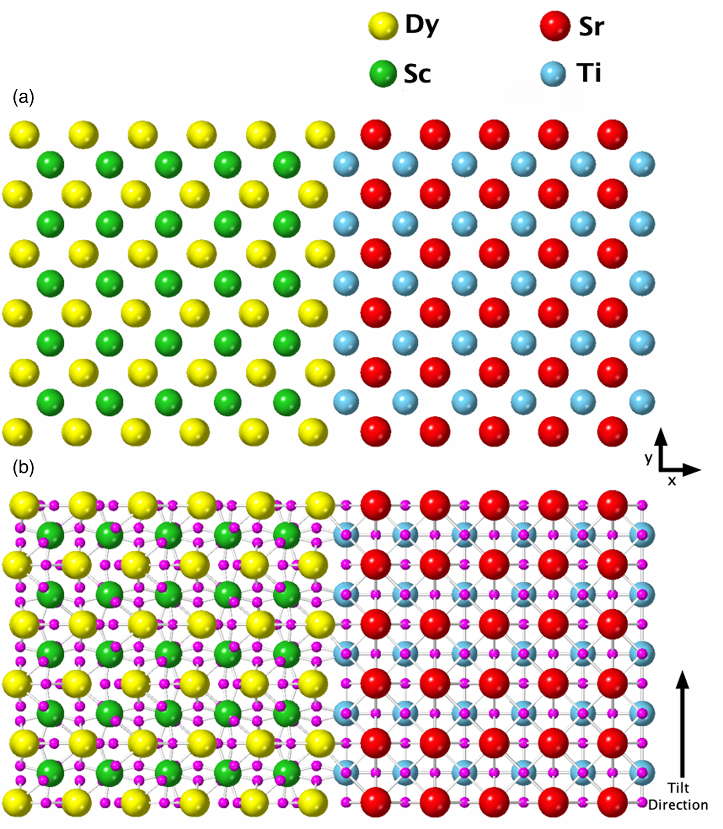
Fig. 1. Crystal structure for an atomically sharp DSO–STO interface, with Dy (yellow) and Sc (green) on the left-hand side of the image and Sr (red) and Ti (blue) on the right-hand side of the image. Here, the structure is shown down the 〈100〉 zone axis with respect to the STO lattice. The DSO lattice is slightly tilted away from the 〈110〉 zone axis in order to have a continuous metallic lattice across the interface, as has been seen experimentally. Oxygen atoms (in pink) have been excluded from (a) to make the metal atom lattice structure clearer to see but are included in (b) to demonstrate the alignment with Ti columns.
The microscope parameters were based on a Thermo Fisher Titan G2 80-300 operating at 200 kV, with a Super-X four-quadrant detector geometry (producing a nominal X-ray collection solid angle of 0.7 srad) and a high-angle annular detector spanning 70–150 mrad. Most simulations assume an aberration-free electron beam with a convergence angle of 25 mrad, but where direct quantitative comparison between simulations and experiment was sought, a 21 mrad convergence angle was used. Integration was carried out over all subshells; only K-lines were simulated for oxygen and only L-lines for dysprosium, and both sets of lines were simulated for the remaining elements, namely, scandium, titanium, and strontium.
The thermal vibration of atoms was incorporated based on a Gaussian-distributed mean square displacement (MSD) of the atoms from their perfect crystal structure. The MSDs were taken from Liferovich & Mitchell (Reference Liferovich and Mitchell2004) for DSO and Abramov et al. (Reference Abramov, Tsirelson, Zavodnik, Ivanov and Brown1995) for STO assuming room temperature and bulk crystal properties. Oxygen atoms on either side of the interface were treated separately and given the MSD for the corresponding compound. In the QEP model, 50 atomic configurations were generated from the above distributions. A Gaussian blurring, with a full width half maximum (FWHM) of 0.08 nm (LeBeau et al., Reference LeBeau, Findlay, Allen and Stemmer2010), was applied to the simulated images to account for finite source size effects. This source size was selected as a typical value for the microscope setup used, which provides a good visual comparison between experiment and simulations. Our integration-based metrics are largely insensitive to subtle variations in effective source size (MacArthur et al., Reference E H, MacArthur, Pennycook, Okunishi, D'Alfonso, Lugg, Allen and Nellist2013). Finally, any line profiles included in the results were calculated by integrating over a unit cell (averaging over multiple unit cells) parallel to the interface (y direction in Fig. 1). For comparison between simulations and experiment, images were converted to an absolute scale in units of counts/s/nA/srad using equation (1) (Chen et al., Reference Chen, Weyland, Sang, Xu, Dycus, LeBeau, D'Alfonso, Allen and Findlay2016).
 $$\displaystyle{N \over {I_{\rm e}\tau }} = F_{{\rm ion}}( {t, \;\;X_{{\rm abs}}} ) \omega \left({\displaystyle{{\rm \Omega } \over {4\pi }}} \right)\varepsilon _{\rm i}$$
Here, N is the number of X-ray counts, I e is the incident beam current, and τ is the dwell time. The term F ion(t, X abs) is calculated using the μSTEM code and is the fraction of the incident electrons that result in ionization for a given thickness t of material and X-ray absorption, X abs. No absorption effects were applied to these simulations. The fluorescence yield is denoted by ω, and we used the values given in Table 1 (Kaye & Laby; Bailey & Swedlund, Reference Bailey and Swedlund1967). The detector solid angle is denoted by Ω and is kept at one for normalized count simulations. For direct comparison between experiment and simulations, a solid angle calculation is required; the Super-X EDX detector Ω is typically quoted as 0.7 srad. However, here, we have made use of the numerical modelng by Xu et al. (Reference Xu, Dycus, Sang and LeBeau2016, Reference Xu, Dycus and LeBeau2018), which takes into account additional shadowing or absorption from the holder and can have a notable effect on the resulting effective solid angle, as shown in Table 1. In Table 1, we only present the effective solid angles for zero stage tilt; however, for the quantification of the experimental data, the exact stage tilt was used and the solid angle adjusted accordingly. Lastly, ɛ i is the detector efficiency for each elemental line, and these are relatively close to one for the majority of the lines investigated here, as can be seen in Table 1 (FEI, 2010).
Table 1. A Summary of all the X-ray Lines Being Investigated and Their Corresponding Calibration Factors Needed for Quantification or Comparison Between Simulation and Experiment.
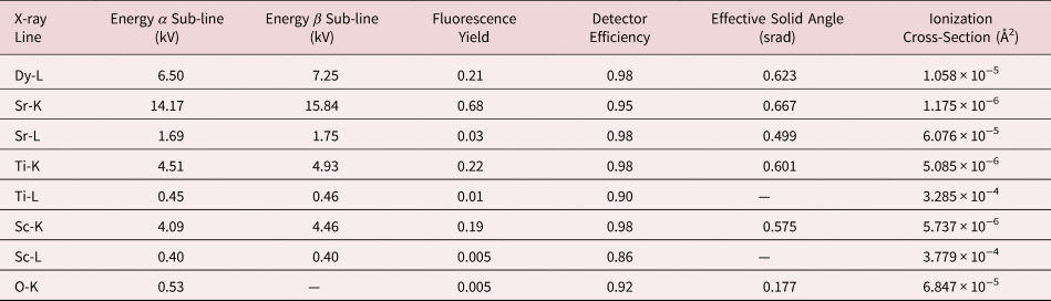
The effective solid angle is presented here for zero stage tilt in both alpha and beta axes. The ionization cross sections are taken from μSTEM.
Alternatively, where specified, intensity was converted to the number of atoms using the partial ionization cross-section method, as previously described (MacArthur et al., Reference MacArthur, Brown, Findlay and Allen2017). In brief, a single atom of each element was simulated in the center of a large unit cell with matching parameters. The large multilayer simulations were then divided by the integrated intensity from this single atom to yield a number of atoms. Note that this number of atoms will not be true in the cases of channeling (MacArthur et al., Reference MacArthur, Brown, Findlay and Allen2017), but this strategy does facilitate comparison with experimental data that has been quantified by linear methods.
Experiments
The experimental data were collected on a DSO-STO multilayer with DSO of varying thicknesses. These DSO/STO multilayers were grown by pulsed laser deposition at 800 °C on Si (100) wafers (more details are set out by Luysberg et al. (Reference Luysberg, Heidelmann, Houben, Boese, Heeg, Schubert and Roeckerath2009)). A TEM lamella was manufactured primarily with an FEI Helios NanoLab 400S and later thinned with an FEI Helios Nanolab 650 dual beam microscope. For the lamella, after extraction from the bulk sample and capping with a 2 mm protective Pt layer, the lamella was thinned down to ~300 nm with a 30 kV Ga ion beam. The sample was further thinned to ~200 nm using an 8 kV beam. A final cleaning step was performed at 2 kV to further reduce the thickness of the amorphous layer caused by the ion beam on the sample sides and to reach the final sample thickness (~125 nm). The lamella was fixed to a Cu Omniprobe half-grid. This half-grid was loaded into the sample holder such that the main tilt was accommodated with alpha tilt, as this is typically more stable than the beta tilt direction.
The experimental maps were obtained using a Thermo Fisher 80–300 kV probe-corrected Titan with a four-quadrant Super-X EDX detector. The microscope was operated at an accelerating voltage of 200 kV, probe convergence angle of 21 mrad and probe current 28.3 pA. Maps were acquired at four different tilts which were nominally at 0°, 1°, 2°, and 3° from the low order 100 zone axis, tilting parallel to the interfaces (see arrow in Fig. 1). EDX maps were acquired using the Velox software with a 512 × 512 frame size and a 10 μs live time, per pixel, per frame and with multiple fast frames accumulated until the sample drifted out of the maximum range for the drift compensation (typically this was after 600–700 frames), resulting in the total electron dose of 3.5–4.2 × 10¹⁰ e/Å2. Acquisition for each tilt was not taken on exactly the same area due to x and y shifts during tilting but it was close and covered the same layers in terms of the x-direction, even if there was some unavoidable y-shift. Electron energy loss spectra were recorded close to the layers to determine sample thickness from t/λ based on the theoretical value of lambda from Malis (Malis et al., Reference Malis, Cheng and Egerton1988) of 102.8 nm. The measured thicknesses were 140 nm, 160 nm, 150 nm, and 130 nm for 0°, 1°, 2°, and 3° tilts respectively. The thickness analysis also indicated a wedge angle of around 0.16°.
The individual ADF STEM and EDX frames were extracted from the series using Hyperspy (de la Peña et al., Reference de la Peña, Prestat, Fauske, Burdet, Jokubauskas, Nord, Ostasevicius, MacArthur, Sarahan, Johnstone, Taillon, Lähnemann, Migunov, Eljarrat, Caron, Aarholt, Mazzucco, Walls, Slater, Winkler, Martineau, Donval, McLeod, Hoglund, Alxneit, Lundeby, Henninen, Zagonel and Garmannslund2019) and recombined using nonrigid registration (Yankovich et al., Reference Yankovich, Berkels, Dahmen, Binev, Sanchez, Bradley, Li, Szlufarska and Voyles2014, Reference Yankovich, Zhang, Oh, Slater, Azough, Freer, Haigh, Willett and Voyles2016) to correct the image distortions and misalignment of atomic columns present within each series. All maps were acquired at atomic scale, so that atomic resolution maps can be extracted (see Fig. 2). However, to treat the spectra accurately (with curve fitting and background subtraction), integration or binning was performed after the nonrigid registration but prior to any additional processing of the EDX spectra. This was done for the line scans where integration was performed parallel to the interface, including all pixels in the field of view. It is worth noting that binning of the experimental data should always be carried out as the first processing step, because it improves the total SNR and, therefore, improves the accuracy of curve fitting or background subtraction. Integration after extraction of counts does not provide the same benefit, because the background subtraction would be performed on the noisier spectra. After binning, a PCA denoising step was performed and the full data set recombined from four fitted components. A model fitting was then applied to the denoised dataset to extract the final X-ray maps. Binning, PCA and curve fitting were all performed using Hyperspy (de la Peña et al., Reference de la Peña, Prestat, Fauske, Burdet, Jokubauskas, Nord, Ostasevicius, MacArthur, Sarahan, Johnstone, Taillon, Lähnemann, Migunov, Eljarrat, Caron, Aarholt, Mazzucco, Walls, Slater, Winkler, Martineau, Donval, McLeod, Hoglund, Alxneit, Lundeby, Henninen, Zagonel and Garmannslund2019).
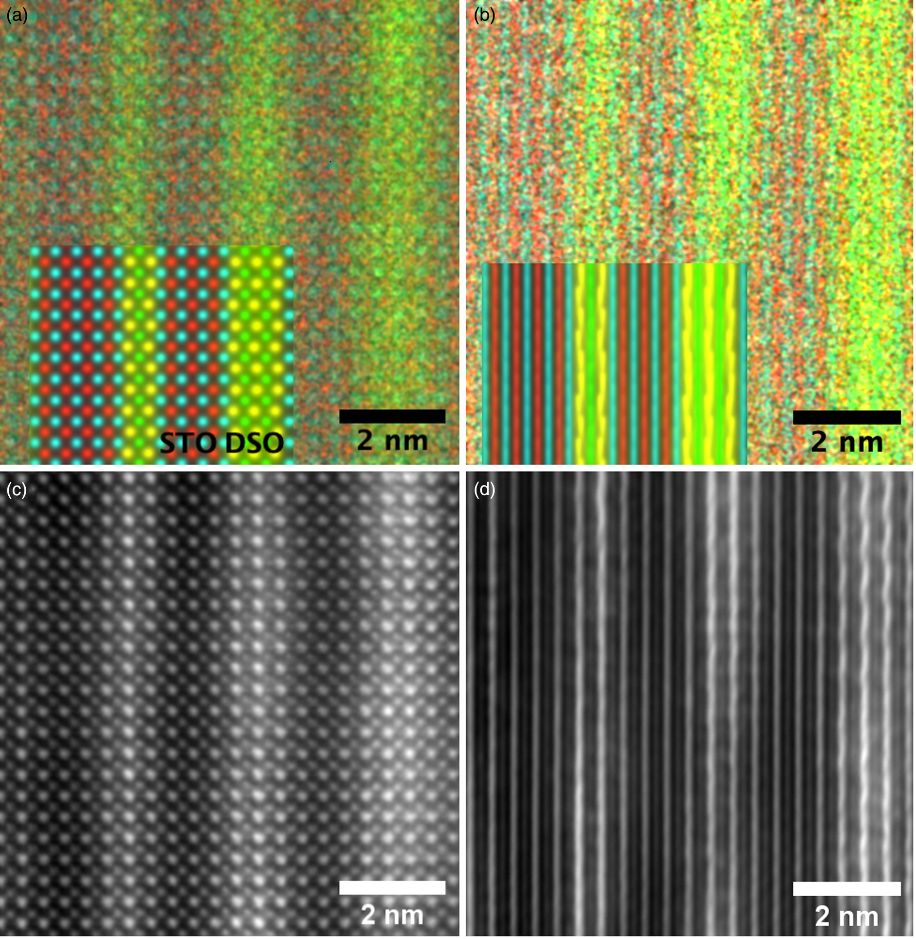
Fig. 2. Experimental atomic resolution EDX map of the multilayer structure at a 0° tilt with the simulation result inset (a) and the experimental atomic EDX maps at 3° tilt with the simulation result inset (b). The metal X-ray signals are overlaid in the following colors: the Dy-L is yellow, Sc-K is green, Sr-K is red and Ti-K is blue. The corresponding ADF images are shown in (c) and (d). An arbitrary intensity scale has been used in this figure. DSO layer thickness increases from left to right.
Intensity maps were then converted to the number of atoms based on the theoretical ionization cross sections in Table 1 and the maths outlined below [equations (2)–(5)], starting from the theoretical equation for X-ray emission in the thin film approximation (Watanabe & Williams, Reference Watanabe and Williams2006):
 $$I_{\rm i} = N_{\rm v}I_{\rm e}\tau N_{\rm e}\rho t\cdot \displaystyle{{Q_{\rm i}\omega _{\rm i}\alpha _{\rm i}\epsilon _{\rm i}} \over {eM}}\cdot \displaystyle{{\rm \Omega } \over {4\pi }}C_{\rm i}$$
N v is Avogadro's number, N e is the number of electron counts in a unit electric charge, ρ is the material density, t is the sample thickness, Q i is the ionization cross section, ω i is the fluorescence yield, α i is the relative transition probability, M is the atomic weight, and C i is the composition in weight fraction. Using the definition for electron dose (D e), equation (3), and the definition for the number of atoms of a given element (N i), equation (4), we can then determine the number of atoms per pixel or per illumination area using equation (5).
 $$D_{\rm e} = \displaystyle{{I_{\rm e}\tau N_{\rm e}} \over {A_{\rm p}}}$$
 $$N_{\rm i} = \displaystyle{{\rho tN_{\rm v}} \over {M}}\cdot C_{\rm i}A_{\rm p}$$
 $$N_{\rm i} = I_{\rm i}\cdot \displaystyle{{4\pi } \over {{\rm \Omega }\epsilon_{\rm i}}}\cdot \displaystyle{e \over {Q_{\rm i}\omega _{\rm i}\alpha _{\rm i}D_{\rm e}}}$$
Here A p is the illumination area (often approximated to the probe area). It should be noted that equations (1) and (2) are equivalent once integration over an atomic column or region of interest has been performed. In this case, F ion = N iQ i. Both equations have been used here to help bring experimentalists and theoreticians together. α i is missing from equation (1), because an integration over all sublines is assumed, whereas equation (2) assumes only one subline is being investigated. Here we have integrated over all sub-lines to maximize signal-to-noise.
Finally, absorption correction was investigated during this research, however it appears that a basic linear absorption does not apply well to atomic EDX data involving electron channeling. As such, it was excluded from the results published here until a more accurate approach is devised. An absorption correction would be expected to increase the number of X-ray counts in the experimental results and, therefore, measured atom counts. The x-rays with energies characteristic of titanium and scandium K-lines are expected to absorb to a greater extent than the x-rays characteristic of the dysprosium and strontium lines. For a single side entry detector with an elevation angle of 35° and a uniform sample thickness of 125 nm the largest absorption correction factor, for the lowest energy x-rays (Sc-K), is 1.0317. Therefore, we expect absorption correction to only change the values presented here by less than 3%. Tilting by 3° would result in a sample thickness increase of 0.14% and a reduction in the beam path to the detectors by 4.5% which would result in a 6.5% change in the absorption correction factor. The experimental tilt applied here is as small as those often used to find the zone axis in TEM specimen, and therefore, additional tilting will have minimal effect on the amount of absorption, provided the resulting take off angle to the detector(s) is still known.
Results and Discussions
Two-Dimensional Images to Line Profiles
We take, as our starting point, the full elemental maps in Figures 2 and 3, showing the elemental distributions in both x and y. These maps show us qualitatively the location of the DSO and STO layers within our specimen. Figure 2 shows the multicolored overlay of elemental maps for experimental images taken at 0° tilt (a) and 3° (b) with the corresponding image simulation inset. Figure 3 shows the raw output image simulations for elemental lines at a 0° tilt. As expected, the resulting simulated X-ray maps (for the metallic elements) are sharply peaked at the atomic columns containing each element, see Figure 3, producing the interlinking sublattice pattern in the combined color map image, Figure 2a, which turns into atomic lines with sample tilt, Figure 2b. The Dy atoms are staggered, producing an oscillating lattice plane when the sample is tilted, which will cause a broadening of the peaks when integrated to a line profile.
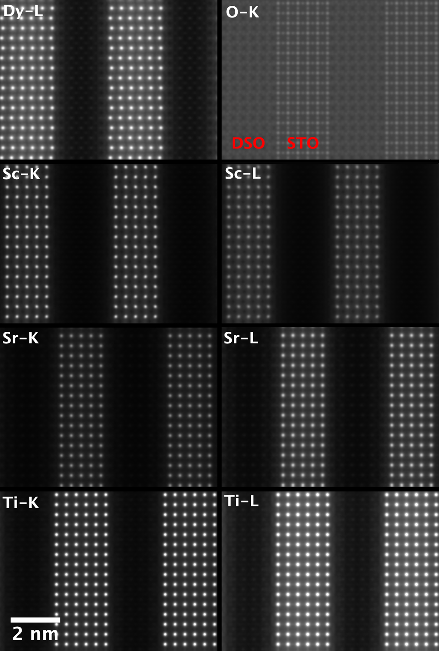
Fig. 3. On-axis maps for each of the simulated elemental lines on a common intensity scale (except the O-K image, which has been multiplied by a factor of two to make the structure details more visible). The regions of DSO and STO have been labeled in red on the O-K image for clarity of layer the locations.
In Figure 3, we can see a halo effect around each of the atomic column sites, suggesting that there is a leakage of intensity across the interface. It is also possible to qualitatively see how the L-lines are less tightly bound to the atomic sites than the K-lines by comparing the FWHM of the peaks. This difference impacts upon how much the resulting signals are affected by electron channeling and, therefore, the measured composition over an interface if different families of lines are used for the different elements.
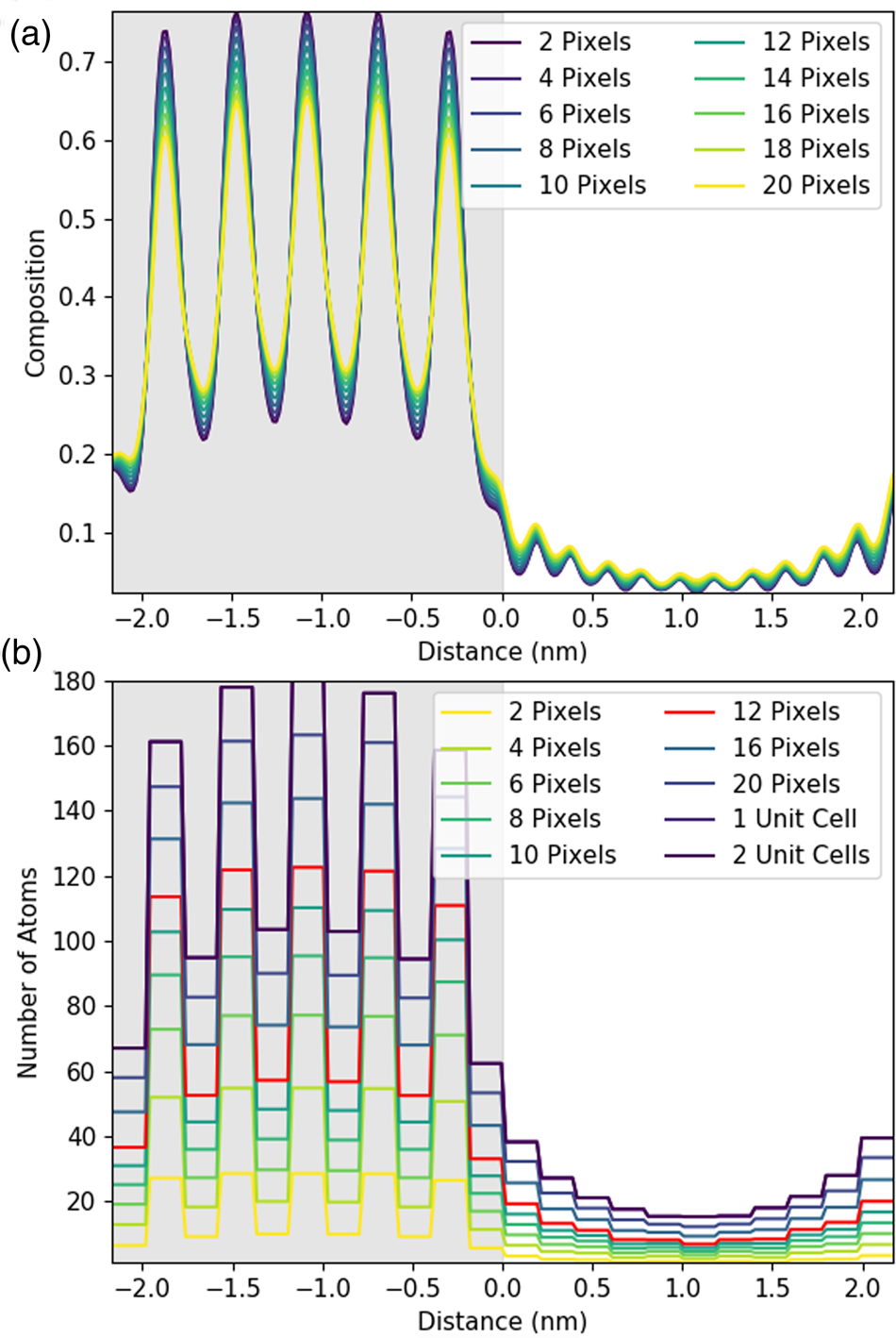
While these two-dimensional maps provide valuable structural insights, they do not help with quantitative measurements. A line profile is far more useful when seeking to determine composition across the interface. The gain from integrating or averaging parallel to the interface for experimental data is clear: an improved signal-to-noise. When only composition information across the interface is sought, the second dimension is anyway redundant. However, it is worth establishing if such a step would always be beneficial when one is not limited by SNR. A series of simulated line profiles with an increasing line width were investigated to see what effect integration has on both accuracy and resolution. Figures 4a and 4b show the changes in X-ray composition and counts, respectively, with an increasing integration width of a line profile for the Sr-K line. In this instance, one atomic plane is ~11.75 pixels and one full lattice spacing is two atomic planes or 23.5 pixels, though integration was applied only to full pixels.

Fig. 4. Understanding the effect of integration in one direction using simulated line profiles. Line profiles here are shown for the Sc-K line with an increasing amount of integration parallel to the interface. The gray region represents the location of the DSO layer. The figure shows integration over one atomic plane with an increasing line thickness in pixels plotted as composition (a) and as the number of atoms in (b) for a 100 nm thick sample. In this instance, one atomic plane is 11.75 pixels, and, therefore, the 12-pixel integration has been highlighted in red. One unit cell is two atomic planes or 23.5 pixels, labeled as 1 unit cell in (b).
Figure 4a shows that the composition profile broadens with integration. The composition here is determined by dividing the number of atoms of Sr implied per pixel—see equations (1), (5), and the associated discussion—by the total number of metal atoms per pixel (oxygen is excluded). The known composition input to the simulation is either 0 or 1 in the STO layer, as the structure alternates between pure Sr columns and pure Ti columns. However, in Figure 4a, the intensity varies only between 0.25 and 0.75, meaning that 25% of the X-rays detected come from Ti (Dy or Sc) columns even when the beam position is located on a Sr column. This is an expected consequence of probe scattering and spreading [see, for example, Kotula et al. (Reference Kotula, Klenov and Von Harrach2012)] and as such can be regarded as a loss of resolution (atomic-scale detail not providing purely atomic column-by-atomic column information). Furthermore, the contrast decreases with increasing integration, dropping down to 0.3 and 0.65. This additional loss of resolution would not happen if our elemental maps could be represented by a series of Gaussians.Footnote 2 A closer examination of Figure 3 reveals high intensity between neighboring columns of the same type, a deviation from what would be expected of 2D Gaussian profiles and the cause of this additional resolution loss. That said, the reduction in contrast from integration is relatively small.
When we convert X-ray signals to atom counts, it is, of course, necessary to integrate over a whole number of columns; therefore, Figure 4b is a lot blockier in presentation than Figure 4a. Here, the data is presented with each horizontal line indicating an integrated intensity for a particular atomic column, and the length of each horizontal line demonstrating the width that has been integrated over. Importantly, if perhaps unsurprisingly, integration over one lattice plane (highlighted in red in Figure 4b) yields about 30% fewer atom counts than integration over a full until cell (two lattice planes). Therefore, the signal for one atomic column is extending further than just one Voronoi integration cell would suggest. This has the biggest implications across the interface, where the amount of signal spreading over the interface also increases with increasing integration. Therefore, while integration improves the absolute number of counts, it comes at a small cost in resolution. (An even higher broadening of the intensity profile is expected for the Dy-L line due to the slight zigzag of the Dy columns seen in the y direction in Figure 3, producing an additional resolution loss.) This loss of resolution, particularly across the interface, should be borne in mind in what follows. Nevertheless, on experimental data, we still consider that integrating parallel to the interface will be worthwhile for the signal-to-noise gain it provides.
Evaluation of Simulated Line Profiles
For the remainder of the paper, we will focus on unit-cell-averaged line profiles, pushing toward accuracy and interpretability. By accuracy, we want to know how closely the measured values, both composition and atom counts, reflect the crystal structure being evaluated. By interpretability, we mean the degree to which EDX signal spreading across the interface reflects true intermixing of elements rather than beam broadening or scattering. A more interpretable map is also a map where the EDX signal before and after the interface is uniform such that the region where the interface exists is easily observable. In earlier work (MacArthur et al., Reference MacArthur, Brown, Findlay and Allen2017), we demonstrated how a deliberate small sample tilt away from the low-order zone axis can suppress the electron channeling and improve the accuracy of quantification via linear methods. Here, we look at sample tilt parallel to the interface. Figure 5 shows the composition profiles for both thick (100 nm) and thin (24 nm) samples. Each row of figures relates to a different sample tilt (0°, 3°, and 5°) and each figure compares two different crystal structures—an abrupt interface (solid lines) and one where 10% intermixing was applied (dashed lines). In what follows, we will be particularly interested in the intensity leaking across the interface for the thick (100 nm) samples. Table 2 summarizes the intensity loss of the last column before the interface (gray) and the intensity gain of the first column after the interface (white).
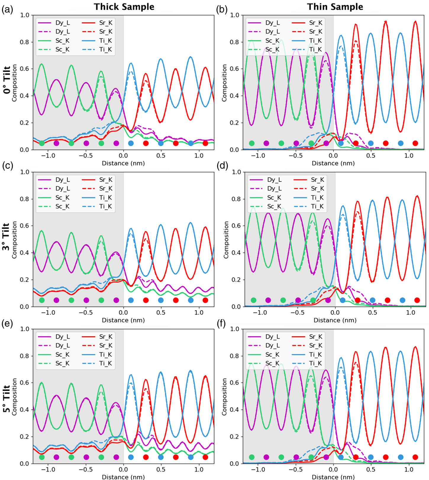
Fig. 5. The effect of beam spreading on the observed sharpness of the interfaces. Simulations presented here from the 24 nm-thick sample (in the right column) and the 100 nm-thick sample (in the left column). The gray region represents the location of the DSO layer and the dots represent the atom column locations for each element. The simulations with 10% interfacial mixing are plotted using dashed lines, while the abrupt interface simulations are in solid lines. A comparison between 0°, 3°, and 5° sample tilts demonstrates the improvement of interpretability in the tilted results as the maxima of the columns before and after the interface become closer to the same height. A small drop in the intensity of the last columns before the interface is the main visible sign of any composition change but could be lost in the beam-spreading effects.
Table 2. Summary of the Intensity Leaking Across the Interface for the 100 nm Simulations.
No Mix and Mix refer to whether or not the interface is abrupt or if 10% intermixing has been incorporated. This table shows the intensity loss of the last full column (or 90% full for the 10% mixing case) before the interface (highlighted in grey) and the intensity gain of the first column (empty or containing 10% atoms for the 10% mixing case) after the interface (highlighted in white). All values are the percentage of the integrated signal intensity taken from peaks in the middle of the layers.
The problem of not reaching the true composition persists for all line profiles. It is notably worse for the thicker specimen as the beam is spreading out and more cross talk occurs with increasing sample thickness. Moreover, there is a certain amount of signal “leaking” across the interface even for the input structure containing an atomically sharp interface. In Figure 5, for the 24 nm-thick calculations (referred to as the thin sample in the figure), the last atomic columns before the interface demonstrate a slightly reduced intensity, ranging between 2 and 4% reduction in measured composition from the integrated signal, when compared with the maximum in the middle of the layer. Likewise, a residual intensity can be seen extending beyond the interface, ranging between 9 and 10%. Further away from the interface, there are notable oscillations in the line profile that coincide with the location of atomic column sites within the next layer. This leaking of intensity is unsurprisingly worse for the thicker sample, as seen in the right-hand side of Figure 5, where the intensity loss of the last column before the interface is 5–7% and additional intensity after the interface is 11–17%, depending on the element selected (see Table 2). This apparent “interface width” is in agreement with experiments by Spurgeon et al. (Reference Spurgeon, Du and Chambers2017), where they determined that a measurement error was preventing them from accurately measuring the true concentration gradient occurring at an interface. Essentially, the original composition profile in the structure of the sample is being imaged by an electron beam that additionally spreads and scatters within the sample. Therefore, understanding how much the beam will spread within the specimen is critical to determining accurate composition profiles within it.
After tilting, several things happen. For the thick specimen, the intensity loss before the interface (see gray values in Table 2) becomes less for all elements other than Dy (ranging between 3 and 6%), but the intensity gain after the interface (see white values in Table 2) becomes higher (ranging between 12 and 16%). It seems, therefore, that the L-line of Dy is very detrimentally affected by tilting, as the signal extending beyond the interface increases with the sample tilt. The K-lines are more robust to the sample tilt: the X-ray signal extending beyond the interface remains rather constant with the tilt (values summarized in Table 2). For the thin specimen (not shown in Table 2), both the intensity loss and the intensity gain increase slightly with the sample tilt. In both samples, there is a gain in the interpretability of the line profiles: the relative heights of the peaks are better aligned so it becomes easier to notice the long-range composition variation. For the thin specimen at zero tilt, the maxima of the Sc peaks lie above those of Dy and the maxima of the Sr peaks are higher than those of Ti. This difference is almost eliminated by a 5° tilt, making the interpretation of composition across the interface easier. Because the peak heights further away from the interface drop down more than those beside the interface, it results in the interface appearing more abrupt. However, the signal leaking across the interface does increase. This is shown in Figure 6, where several tilts (replotted from Figure 5) for the 100 nm sample are shown on the same figure for only the Sc-K and Ti-K lines.

Fig. 6. The effect of beam spreading on the observed sharpness of the interfaces. Here, the data from the 100 nm sample is replotted from Figure 5 to show only the Sc-K ad T-K lines at tilts of 0° and 5°. The colored dots present the atomic column locations of every element, and the gray-shaded region shows the location of the DSO layer.
A measured interfacial width that is dependent on sample thickness will complicate the extraction of real composition profiles. As an example of a more diffuse interface, 10% mixing was introduced into the simulations to see how visible such a profile is relative to the effects of probe scattering and spreading, and the resolution loss from integration. These results are included as dashed lines in Figure 5. For the thin specimen, interfacial mixing can be spotted at all sample tilts (Figs. 5b, 5d, 5f), especially when compared side by side with the unmixed case. However, for the thicker specimen, such a small amount of intermixing is easily lost due to the increased beam broadening, Figures 5a, 5c, and 5e. This is more easily demonstrated when looking at the composition change between mixing and no mixing for the Dy-L line in Table 2. After 10% mixing, a 2% change in composition is seen at the last column before the interface. In fact, the absolute values in Table 2 change very little with the sample tilt for all X-ray lines; however, the relative height of the K-lines becomes closer together. The difference between the unmixed and the mixed results changes the leaked intensity values by less than 3% on average. This is because we see more of a vertical shift in each of the individual lines rather than changes in their relative shapes.
Aside from the sample tilt, another parameter open to selection by the users is which line to use for quantification. Historically, K-lines are used in preference to L- or M-lines for a given element, because they are of higher energy and will be absorbed less before escaping the sample (Watanabe & Williams, Reference Watanabe and Williams2006). Additionally, when it comes to using calculated ionization cross-sections, the K-transitions are better understood and easier to model, whereas this accuracy drops off significantly for the lower energy transitions. This also means that the fluorescence yields are typically more reliable for K-lines. However, the dysprosium K-line (at 46 keV) is too high in energy to be recorded in normal operating conditions. In Figure 7, the K-lines are dashed, while the L-lines remain solid such that we can compare the accuracy of the different lines. Although the line profiles have been integrated such that values are now per atomic column, it is still possible to make some analysis of signal localization. Before integration, a comparison can be made about widths and heights of the peaks; after integration, we are now looking at volumes. The K-lines, owing to the fact that they originate from a more tightly bound orbital, seem to be more strongly affected by electron channeling, which leads to a much higher number of atom counts after quantification at zero tilt, see Figure 7a. In particular, the lighter elements (Ti, blue, and Sc, green) show far higher intensity that would erroneously lead to assuming higher composition in what is actually a stoichiometric structure with a ratio of 1:1. To put it another way, the ratio between the peak of Ti columns to Sr columns is 4:3, so one could erroneously expect 25% more Ti atoms within the system. This difference is stark for the K-lines, but is still present for the L-lines. With the sample tilt, the difference between two X-ray lines for the same element reduces, giving us a Ti:Sr peak ratio of 6:5 although its seems that they never fully overlap, at least for scandium and titanium. In the presence of notable absorption, this peak ratio would serendipitously look better, because the Ti-K line would suffer more absorption than the Sr-K with a similar case for Sc-K and Dy-L.
Fig. 7. The effect of line selection on quantified column-by-column line profiles. The gray region represents the location of the DSO layer. The composition was determined from the quantification of only K-lines (excluding Dy where the L-line was used because no K-line exists in the investigated energy range) or of L-lines (dashed lines on the figures). (a) and (b) show the number of atom counts at 0° and 5° tilts, respectively. (c) and (d) show the composition per column at 0° and 5° tilts, respectively. There is a higher composition on the columns that should be empty for the L-lines due to increased delocalization of the signal, and a corresponding lower signal in the full columns. There is also a higher signal propagating across the interface; however, this is very small in comparison to the other probe scattering and spreading effects.
After a 5° sample tilt, the L-lines have a larger minimum between atomic rows, which will slightly reduce the visibility of atomic columns during mapping. In the quantitative values on intensity leaking in Table 2, we can see that there are only a few percentage points of difference between the K- and L-lines, with the L-lines leaking more across the interface. However, this additional delocalization due to a line selection is minor in comparison with the overall beam broadening effect.
Looking at composition rather than atom counts, Figures 7c and 7d, these appear to get worse at higher sample tilt, despite the fact that the atom counts get better. This is primarily because of a resolution loss with sample tilt. As channeling reduces, beam broadening becomes the dominating effect within the specimen. Therefore, as we tilt away from a zone axis, column-by-column analysis becomes less reliable. The on-column composition values for Ti, Sc, and Dy all seem to drop with tilt; however, the Sr composition values (red) increase. More importantly, the off-column compositions also drop after tilting, meaning that a unit cell composition will get a realistic answer closer to a 1:1 ratio for each of the layers (ignoring the interface effects). Essentially, the more delocalized our signal, the better our ability will be to quantify absolute values. Therefore, there is a compromise to be made between resolution and accuracy of composition determination.
The focus up until now has been the heavy metal atoms. This is primarily because the oxygen K-line is harder to detect accurately experimentally: it is far more susceptible to absorption and has a lower detection rate. However, the simulated oxygen signal in this system does yield some interesting information worth discussing. The O-K map in Figure 3 looks rather different from the maps for the metals, because it is heavily influenced not only by the location of the oxygen atoms but also by the locations of the metal atoms. In the STO layer, the location of the columns containing Ti atoms is clearly seen as the brightest columns in the O-K signal, a phenomenon previously explained by Forbes et al. (Reference Forbes, D'Alfonso, Williams, Srinivasan, Fraser, McComb, Freitag, Klenov and Allen2012). By contrast, the O-K intensity in the DSO layer is much lower, despite containing exactly the same number of oxygen atoms. This can be explained by the fact that none of the oxygen atoms in this layer are aligned in columns of atoms, with each other, or in a column with one of the heavier metal atoms, which would facilitate electron channeling. A similar effect has also been seen for the nitrogen signal in GaN–AlInN interfaces by Mevenkamp et al. (Reference Mevenkamp, MacArthur, Tileli, Ebert, Allen, Berkels and Duchamp2020). Therefore, the boost in intensity from electron channeling is much lower for the oxygen in the DSO case, and this allows for more reliable quantification even without tilting the sample. The reduced channeling contribution can also be seen by evaluating the O-K line intensity, shown as a function of sample tilt in Figure 8.
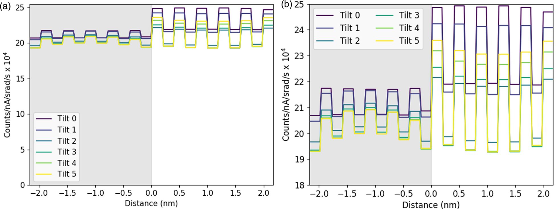
Fig. 8. (a) Integrated line profile showing the O-K signal at different sample tilts. This is on an absolute scale to highlight the relatively minor changes occurring with tilt in comparison with the metal lines discussed above. There is a larger channeling effect in the STO layer, and also a greater change of the signal with sample tilt. (b) shows the same data as (a) rescaled to emphasize the variation with sample tilt. The gray regions represent the location of the DSO layer.
Also seen in Figure 8b is a phenomenon whereby the minimum X-ray intensity is visible for a 2° tilt but then begins to increase again. This phenomenon was seen for all elements investigated. By a 4° and 5° tilt of the sample, there is a rebound in the integrated intensity, before it most likely drops down again at higher tilts still. Such oscillations have been seen by Lugg et al. (Reference Lugg, Kothleitner, Shibata and Ikuhara2015) in the EDX signal and by MacArthur et al. (Reference E H, MacArthur, Pennycook, Okunishi, D'Alfonso, Lugg, Allen and Nellist2013) when looking at the ADF signal intensity.
Comparison of Experiment and Simulations
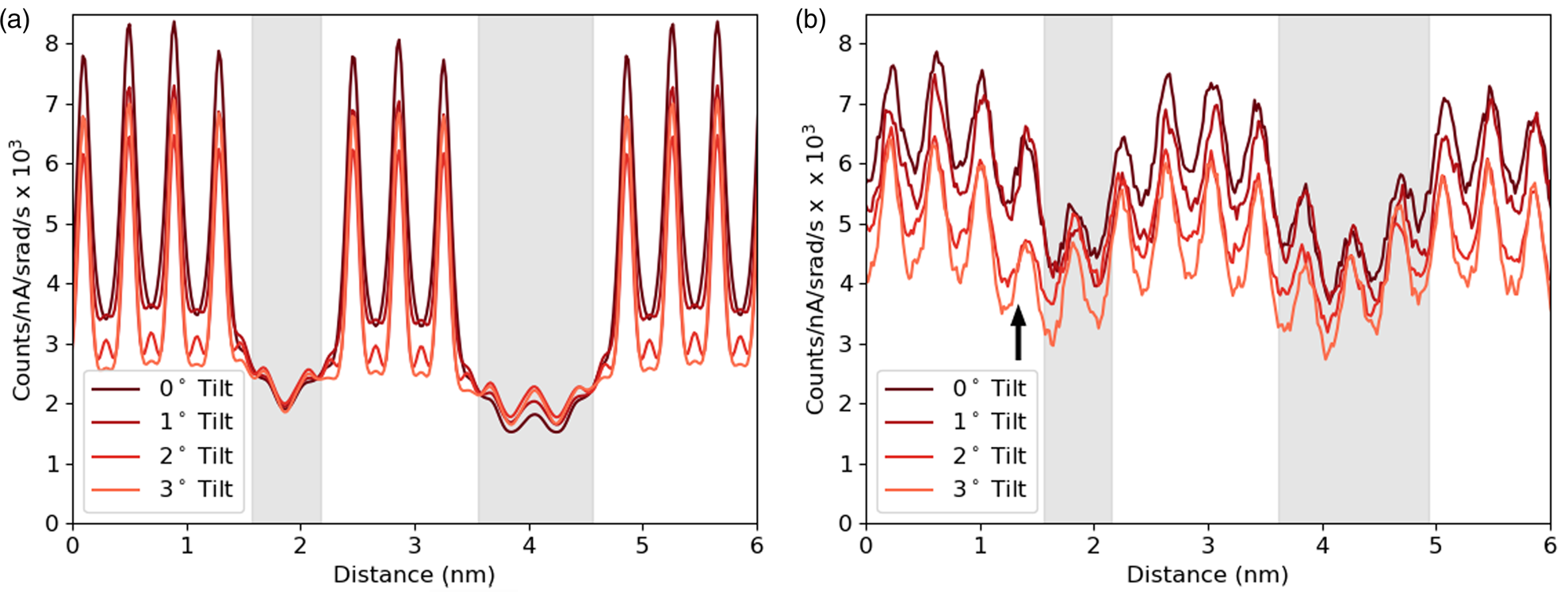
Having developed through simulation some understanding of the expected accuracy and interpretability of the line profiles of interfaces, we can start making comparisons with an experimental example. The first comparison shown in Figure 9 focuses on one element, Sr-K, and looks at how the line profile varies with sample tilt. Here a slightly modified structure file has been used for simulations with a smaller layer width for the DSO layers, and a sample thickness of 124.7 nm was found to be the closest match. Although there is a match in the average intensity, the contrast of the experiments is significantly lower. The same drop in intensity with sample tilt can be seen in both the experimental and simulated results. This is important because, without channeling, one would expect the signal to increase with sample tilt for a lamella sample due to an increased thickness in the beam direction and a reduced shadowing from the holder (see Slater et al., Reference Slater, Camargo, Burke, Zaluzec and Haigh2014). The greatest change occurs during the first two degrees of tilt, which is consistent with our simulations. Not only do the peak intensities drop significantly with tilt as the amount of electron channeling reduces, but there is some drop in the values between the peaks, meaning some atomic-scale contrast is preserved. There appears to be a small drop in the overall intensity from left to right in the experimental results. However, from the EELS thickness measurements, the angle of the FIB wedge was 0.16°, making thickness variation an unlikely cause. What seems more likely is that the beam broadening effect increases with an increasing thickness of the DSO layers, allowing the Sr signal to drop more during each layer. It is worth noting the “missing” atoms visible around 1.5 nm (highlighted with an arrow) in Figure 9b. As mentioned in the Experimental Methods sections, there was a degree of x–y shift during sample tilting, and while every effort was made to minimize this and return to the same area there could be some remnant y-shift (parallel to the interface). Therefore, this sudden drop of intensity or missing atoms seen here for the 2° and 3° tilts is simply due to imaging an area where the DSO layer is thicker by one extra layer of Dy.

Fig. 9. The simulated (a) and experimental (b) line profiles for the Sr-K line at different sample tilts. The simulation is at a thickness of 124.7 nm, and the counts are normalized by electron dose and solid angle. The gray regions represent the location of the DSO layers, which are only approximate for the experimental data.
Next, we examine the combined line profiles for all metallic elements in terms of normalized counts, Figure 10, and in terms of absolute atom counts, Figure 11. The signal in terms of absolute counts has additionally been integrated in the interface direction, such that full atomic planes are included in each integration. First, the quantified line profiles show us the best match between experiments and a simulation of a 124.7 nm-thick specimen, based on both a comparison of normalized counts, Figure 10, and integrated atom counts, Figure 11. The thickness measurements using EELS suggested a sample thickness of ~150 nm on average. There is a 10% error on the mean free path, λ, usually in the direction of overestimation, so this is in reasonable agreement. Second, the Ti-K lines appear around 40% higher than we would expect. The Ti-Kα does overlap with the Sc-Kβ, which is why curve fitting was used for the signal extraction. A more basic linear background subtraction with an additional subtraction of the estimated Sc-Kβ based on the expected Kα/Kβ ratio also showed comparable numbers of counts (within 5%). In the simulations, the Ti curve is distinctly higher than the Sr curve at zero tilt, but this difference reduces with sample tilt. The tilt values for the experimental data are only nominal and may vary by up to 10%; however, this is not enough to account for the shift in the Ti curves. Any error in the Dy-L signal is likely in part due to uncertainties in the ionization cross-section for this element (Xin et al., Reference Xin, Dwyer and Muller2014). However, large variations and problems also occur in the determination of fluorescence yields for this element.
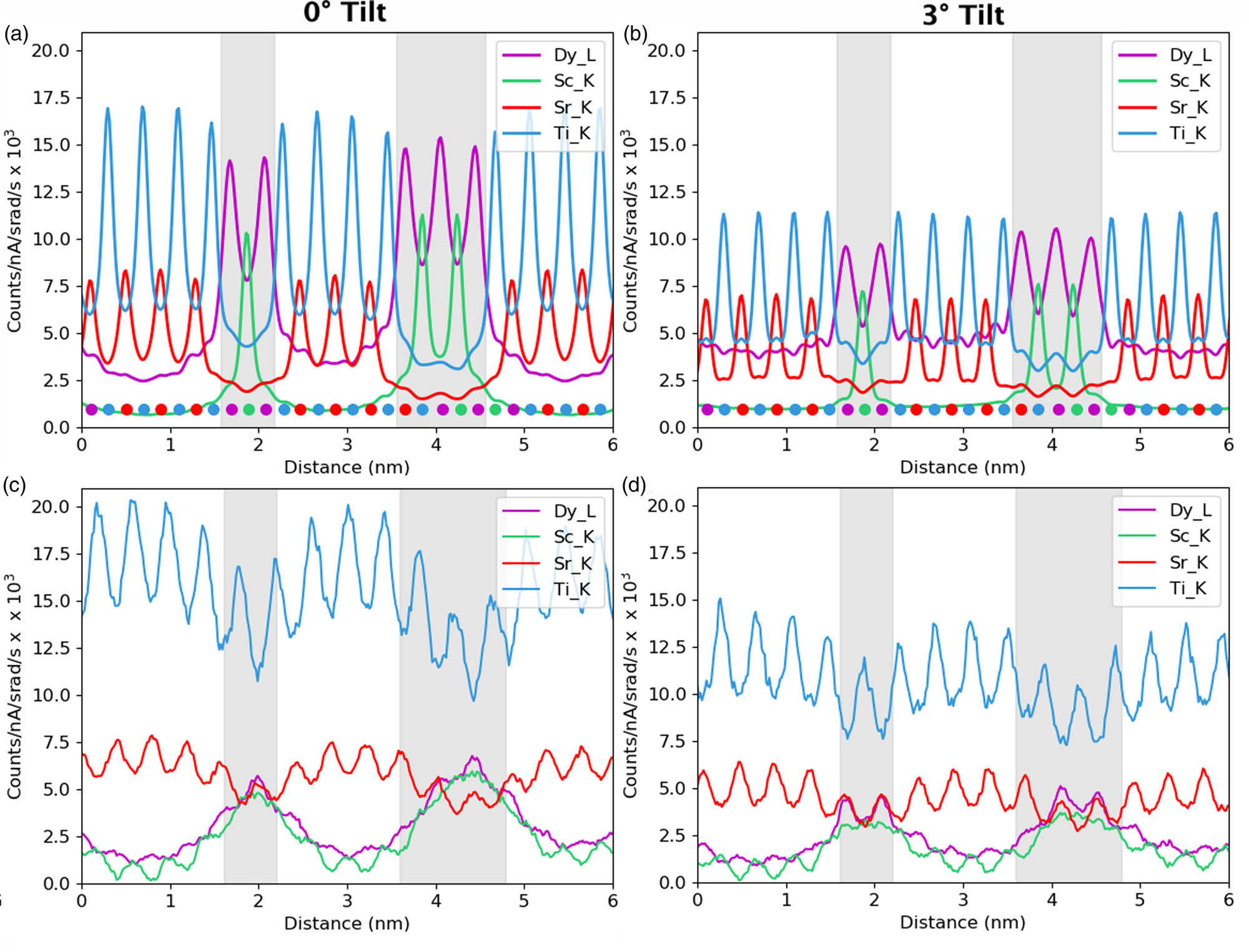
Fig. 10. Simulated atomic line profiles at a 0° tilt (a) and a 3° tilt (b). The equivalent experimental line profiles are shown for the 0° tilt (c) and the 3° tilt (d). The intensity scale of the results are normalized counts. The gray regions represent the locations of the DSO layers, which are only approximate for the experimental data.
Fig. 11. Simulated atomic line profiles at a 0° tilt (a) and a 3° tilt (b). The equivalent experimental line profiles are shown for 0° tilt (c) and 3° tilt (d). The intensity of the results is in number of atoms and have been integrated over a unit cell as the simulations demonstrated this to be the optimum integration range for retrieving atom counts. The gray regions represent the locations of the DSO layers, which are only approximate for the experimental data.
Despite the closeness between the sample thicknesses of both experiment and simulations, it is not possible to conclude whether or not the experimental sample contains an abrupt series of multilayers. The clearness of the Sr and Ti peaks throughout the experimental line profiles in Figure 10 points toward the possibility of layers only partially containing Dy and Sc, because the composition would reach nowhere near 100%. Alternatively, the layer may not be fully formed in the z-direction parallel to the electron beam or there could be steps in the material. However, the STO substrate is known to have a small root mean square flatness of 0.5 nm over a 4 μm2 area (Schaadt et al., Reference Schaadt, Yu, Vaithyanathan and Schlom2004), which allows for the growth of films of similar roughness. Additionally, previous work on these materials by Luysberg et al. (Reference Luysberg, Heidelmann, Houben, Boese, Heeg, Schubert and Roeckerath2009) revealed atomically flat interfaces within the multilayer system. Therefore, we would assume atomically sharp or close to atomically sharp interfaces within the area of investigation. As such, we assume most of the effects seen are due to beam broadening which is exacerbated by such narrow layers in the specimen.
Conclusions
In conclusion, accurate composition determination of a crystalline sample is only possible if steps are taken to reduce and suppress the amount the electron beam channels within the specimen. Therefore, the researcher is left with the dilemma of choosing between beautiful but only qualitative maps, or improved quantification at a cost of resolution. Here, we have shown that, by tilting parallel to an interface and integrating in the same direction as this tilt, the accuracy of the EDX quantification in terms of the absolute number of atoms even over an interface can be significantly improved at only a small cost in resolution. Interpretability is also improved with both sample tilt and integration. With careful calibration of the microscope, it is possible to get absolute atom count values from experimental maps to directly compare with simulated values, allowing true absolute quantification of materials and their composition. Once channeling is suppressed, this can also be treated linearly.
For the specimen thicknesses investigated here (20.7, 100, and 124 nm), there is still an issue with beam broadening and scattering that needs to be better understood to really determine how abrupt an interface is. Simulations can help with this. In particular, it is important to know how much beam broadening to expect for an abrupt interface at the measured sample thickness before it becomes possible to evaluate deviations from this. Small composition changes like 10% intermixing can be significantly smaller than the beam broadening effect and would be lost unless the scattering of the electron beam can be taken into account. Therefore, a naive column-by-column analysis of such data will lead to erroneous results or a measurement error.
Essentially, channeling helps with spatial confinement of the probe, and when we suppress channeling, by a combination of integration and sample tilt, it comes at a cost in resolution. However, this may make it easier to model the beam spreading and broadening within the specimen, which would allow us to more accurately determine composition at an interface. For an accurate determination of composition across an interface the amount of beam broadening within the specimen needs to be calculated such that this effect can be subtracted from the experimental data so as to get back to the underlying composition information.
Acknowledgment
The authors would like to thank Jürgen Schubert for helping to supply the sample and valuable discussions on the topic. K. E. MacArthur and M. Heggen acknowledge the Helmholtz Funding agency and the DFG (grant number HE 7192/1-2) for their financial support of this work. L. J. Allen acknowledges the support of the Alexander von Humboldt Foundation. This research was supported under the Discovery Projects funding scheme of the Australian Research Council (Projects DP140102538 and FT190100619). K.E. MacArthur, A.B. Yankovich and A. Béché acknowledge support from the European Union's Horizon 2020 research innovation program under grant agreement No. 823717 – ESTEEM3. A.B. Yankovich also acknowledges support from the Materials Science Area of Advance at Chalmers and the Swedish Research Council (VR, under grant No: 2020-04986).


 Open access