Hostname: page-component-76fb5796d-wq484 Total loading time: 0 Render date: 2024-04-26T07:26:23.992Z Has data issue: false hasContentIssue false

A Novel Monochromator with Offset Cylindrical Lenses and Its Application to a Low-Voltage Scanning Electron Microscope

Published online by Cambridge University Press:  15 February 2022

Takashi Ogawa*
Affiliation:
Advanced Instrumentation Institute, Korea Research Institute of Standards and Science, 267 Gajeong-ro, Yuseong, Daejeon 34113, Republic of Korea Major in Nano Science, University of Science and Technology, 217 Gajeong-ro, Yuseong, Daejeon 34113, Republic of Korea
Yu Yamazawa
Affiliation:
Hitachi High-Tech Corporation, 882 Ichige, Hitachinaka, Ibaraki 312-8504, Japan
Satoshi Kawai
Affiliation:
Hitachi High-Tech Corporation, 882 Ichige, Hitachinaka, Ibaraki 312-8504, Japan
Atsushi Mouri
Affiliation:
Hitachi High-Tech Corporation, 882 Ichige, Hitachinaka, Ibaraki 312-8504, Japan
Junichi Katane
Affiliation:
Hitachi High-Tech Corporation, 882 Ichige, Hitachinaka, Ibaraki 312-8504, Japan
In-Yong Park
Affiliation:
Advanced Instrumentation Institute, Korea Research Institute of Standards and Science, 267 Gajeong-ro, Yuseong, Daejeon 34113, Republic of Korea Major in Nano Science, University of Science and Technology, 217 Gajeong-ro, Yuseong, Daejeon 34113, Republic of Korea
Yoshizo Takai
Affiliation:
Department of Material and Life Science, Graduate School of Engineering, Osaka University, 2-1 Yamada-oka, Suita, Osaka, Japan
Toshihide Agemura
Affiliation:
Hitachi High-Tech Corporation, 882 Ichige, Hitachinaka, Ibaraki 312-8504, Japan
*
*Corresponding author: Takashi Ogawa, E-mail: togawa@kriss.re.kr
Get access

Abstract

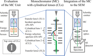
Low-voltage scanning electron microscopes (LV-SEMs) are widely used in nanoscience. However, image resolution for SEMs is restricted by chromatic aberration due to energy spread of the electron beam at low acceleration voltage. This study introduces a new monochromator (MC) with offset cylindrical lenses (CLs) as one solution for LV-SEMs. The MC optics, with highly excited CLs in offset layouts, has advantageous high performance and simple experimental setup, making it suitable for field emission LV-SEMs. In a preliminary evaluation, our MC reduced the energy spread from 770 to 67 meV. The MC was integrated into a commercial SEM equipped with an out-lens (a conventional objective lens without immersion magnetic or retarding electric fields) and an Everhart–Thornley detector. Comparing SEM images under two conditions with the MC turned on or off, the spatial resolution was improved by 58% at 0.5 and 1 keV. The filtering effect of the MC decreased the probe current with a ratio (i.e., transmittance) of 5.7%, which was consistent with estimations based on measured energy spreads. To the best of our knowledge, this is the first report on an effective MC with higher-energy resolution than 100 meV and the results offer encouraging prospects for LV-SEM technology.

Type
Software and Instrumentation
Copyright
Copyright © The Author(s), 2022. Published by Cambridge University Press on behalf of the Microscopy Society of America

Access options

Get access to the full version of this content by using one of the access options below. (Log in options will check for institutional or personal access. Content may require purchase if you do not have access.)

References

Barth, JE & Kruit, P (1996). Addition of different contributions to the charged particle probe size. Optik 101, 101109.Google Scholar
Barth, JE, Nykerk, MD, Mook, HW & Kruit, P (2000). SEM resolution improvement at low voltage with gun monochromator. 12th European Congress On Electron Microscopy, pp. 1437–1438.Google Scholar
Batson, PE, Dellby, N & Krivanek, OL (2002). Sub-ångstrom resolution using aberration corrected electron optics. Nature 418, 617620. doi:10.1038/nature00972CrossRefGoogle ScholarPubMed
Brodusch, N, Demers, H, Gellé, A, Moores, A & Gauvin, R (2019). Electron energy-loss spectroscopy (EELS) with a cold-field emission scanning electron microscope at low accelerating voltage in transmission mode. Ultramicroscopy 203, 2136. doi:10.1016/j.ultramic.2018.12.015CrossRefGoogle ScholarPubMed
Egerton, RF (2014). Choice of operating voltage for a transmission electron microscope. Ultramicroscopy 145, 8593. doi:10.1016/j.ultramic.2013.10.019CrossRefGoogle ScholarPubMed
Erdman, N & Bell, DC (2012). SEM instrumentation developments for low kV imaging and microanalysis. In Low Voltage Electron Microscopy, Bell, DC & Erdman, N (Eds.), pp. 3155. Chichester, UK: John Wiley & Sons, Ltd. doi:10.1002/9781118498514.ch2CrossRefGoogle Scholar
Essers, E, Benner, G, Mandler, T, Meyer, S, Mittmann, D, Schnell, M & Höschen, R (2010). Energy resolution of an Omega-type monochromator and imaging properties of the MANDOLINE filter. Ultramicroscopy 110, 971980. doi:10.1016/j.ultramic.2010.02.009CrossRefGoogle Scholar
Fransen, MJ, Faber, JS, Van Rooy, TL, Tiemeijer, PC & Kruit, P (1998). Experimental evaluation of the extended Schottky model for ZrO/W electron emission. J Vac Sci Technol B 16, 20632072. doi:10.1116/1.590128CrossRefGoogle Scholar
Frosien, J (1989). Compound magnetic and electrostatic lenses for low-voltage applications. J Vac Sci Technol B 7, 1874. doi:10.1116/1.584683CrossRefGoogle Scholar
Hachtel, JA, Huang, J, Popovs, I, Jansone-Popova, S, Keum, JK, Jakowski, J, Lovejoy, TC, Dellby, N, Krivanek, OL & Idrobo, JC (2019). Identification of site-specific isotopic labels by vibrational spectroscopy in the electron microscope. Science 363, 525528. doi:10.1126/science.aav5845CrossRefGoogle ScholarPubMed
Haider, M, Uhlemann, S, Schwan, E, Rose, H, Kabius, B & Urban, K (1998). Electron microscopy image enhanced. Nature 392, 768769. doi:10.1038/33823CrossRefGoogle Scholar
Honda, K & Takashima, S (2003). Chromatic and spherical aberration correction in the LSI inspection scanning electron. JEOL News 38, 3640.Google Scholar
Ibach, H & Mills, DL (1982). Electron Energy Loss Spectroscopy and Surface Vibrations. New York: Academic Press. doi:10.1016/C2013-0-10894-XGoogle Scholar
Ichinokawa, T (1968). Electron energy analysis by a cylindrical magnetic lens. Jpn J Appl Phys 7, 799813. doi:10.1143/JJAP.7.799CrossRefGoogle Scholar
ISO/TS24597 (2011). Microbeam analysis - Scanning electron microscopy - Methods of evaluating image sharpness.Google Scholar
Joy, DC (2005). The aberration corrected SEM. AIP Conf Proc 788, 535542. doi:10.1063/1.2063015CrossRefGoogle Scholar
Joy, DC & Joy, CS (1996). Low voltage scanning electron microscopy. Micron 27, 247263. doi:10.1016/0968-4328(96)00023-6CrossRefGoogle Scholar
Knell, G & Plies, E (1999). Simulation of an improved magnetic–electrostatic detector objective lens for LVSEM. Nucl Instrum Methods Phys Res A 427, 99103. doi:10.1016/S0168-9002(98)01548-4CrossRefGoogle Scholar
Krivanek, OL, Dellby, N, Hachtel, JA, Idrobo, JC, Hotz, MT, Plotkin-Swing, B, Bacon, NJ, Bleloch, AL, Corbin, GJ, Hoffman, MV, Meyer, CE & Lovejoy, TC (2019). Progress in ultrahigh energy resolution EELS. Ultramicroscopy 203, 6067. doi:10.1016/j.ultramic.2018.12.006CrossRefGoogle ScholarPubMed
Krivanek, OL, Lovejoy, TC, Dellby, N, Aoki, T, Carpenter, RW, Rez, P, Soignard, E, Zhu, J, Batson, PE, Lagos, MJ, Egerton, RF & Crozier, PA (2014). Vibrational spectroscopy in the electron microscope. Nature 514, 209212. doi:10.1038/nature13870CrossRefGoogle ScholarPubMed
Kruit, P & Jansen, GH (2009). Space charge and statistical Coulomb effects. In Handbook of Charged Particle Optics, Orloff, J (Ed.), pp. 341389. Boca Raton: CRC Press.Google Scholar
Lagos, MJ, Trügler, A, Hohenester, U & Batson, PE (2017). Mapping vibrational surface and bulk modes in a single nanocube. Nature 543, 529532. doi:10.1038/nature21699CrossRefGoogle Scholar
Luo, T & Khursheed, A (2006). Second-order aberration corrected electron energy loss spectroscopy attachment for scanning electron microscopes. Rev Sci Instrum 77, 043103. doi:10.1063/1.2190208CrossRefGoogle Scholar
Mankos, M, Shadman, K & Kolarik, V (2016). Novel electron monochromator for high resolution imaging and spectroscopy. J Vac Sci Technol B 34, 06KP01. doi:10.1116/1.4962383CrossRefGoogle Scholar
Möllenstedt, G (1949). Die elektrostatische lines als hochauflösender geschwindigkeitsanalysator. Optik 5, 499517.Google Scholar
Mook, H & Kruit, P (2000). Construction and characterization of the fringe field monochromator for a field emission gun. Ultramicroscopy 81, 129139. doi:10.1016/S0304-3991(99)00193-XCrossRefGoogle ScholarPubMed
Mukai, M, Okunishi, E, Ashino, M, Omoto, K, Fukuda, T, Ikeda, A, Somehara, K, Kaneyama, T, Saitoh, T, Hirayama, T & Ikuhara, Y (2015). Development of a monochromator for aberration-corrected scanning transmission electron microscopy. Microscopy 64, 151158. doi:10.1093/jmicro/dfv001CrossRefGoogle ScholarPubMed
Nagatani, T, Suzuki, T & Yamada, M (1986). Direct observation of magnesium oxide crystal by means of a high resolution SEM. J Electron Microsc 35, 208209. doi:10.1093/oxfordjournals.jmicro.a050568Google Scholar
Noh, H, Cho, B, Kim, J & Ogawa, T (2019). Design and aberration study of a new miniature energy analyzer with correctors in a scanning electron microscope. Nucl Instrum Methods Phys Res A 917, 917. doi:10.1016/j.nima.2018.11.087CrossRefGoogle Scholar
Ogawa, T (2019). Evaluation of a monochromator with double cylindrical lenses for electron microscopy. Int J Modern Phys A 34, 113. doi:10.1142/S0217751X19420065CrossRefGoogle Scholar
Ogawa, T & Cho, B (2015 a). A new monochromator with multiple offset cylindrical lenses. Nucl Instrum Methods Phys Res A 772, 513. doi:10.1016/j.nima.2014.10.075CrossRefGoogle Scholar
Ogawa, T & Cho, B (2015 b). A new monochromator with multiple offset cylindrical lenses 2: Aberration analysis and its applications. Nucl Instrum Methods Phys Res A 800, 1828. doi:10.1016/j.nima.2015.08.009CrossRefGoogle Scholar
Ogawa, T, Cho, B & Ahn, SJ (2015 a). A novel monochromator with double cylindrical lenses. Microsc Microanal 21, 112117. doi:10.1017/S1431927615013239CrossRefGoogle Scholar
Ogawa, T, Cho, B & Ahn, SJ (2015 b). Low-energy scanning electron microscope using a monochromator with double-offset cylindrical lenses. J Vac Sci Technol B, Nanotechnol Microelectron 33, 06FJ01. doi:10.1116/1.4931933CrossRefGoogle Scholar
Ogawa, T & Takai, Y (2018). Evaluation of electron optics with an offset cylindrical lens: Application to a monochromator or energy analyzer. J Vac Sci Technol B 36, 032902. doi:10.1116/1.5025775CrossRefGoogle Scholar
Reimer, L (Ed.) (1995). Energy-Filtering Transmission Electron Microscopy. Berlin, Heidelberg: Springer. doi:10.1007/978-3-540-48995-5CrossRefGoogle Scholar
Reimer, L (1998). Scanning Electron Microscopy, 2nd ed. Berlin, Heidelberg: Springer. doi:10.1007/978-3-540-38967-5CrossRefGoogle Scholar
Reimer, L & Kohl, H (2008). Transmission Electron Microscopy, 5th ed. New York: Springer. doi:10.1007/978-0-387-40093-8Google Scholar
Rez, P, Aoki, T, March, K, Gur, D, Krivanek, OL, Dellby, N, Lovejoy, TC, Wolf, SG & Cohen, H (2016). Damage-free vibrational spectroscopy of biological materials in the electron microscope. Nat Commun 7, 10945. doi:10.1038/ncomms10945CrossRefGoogle ScholarPubMed
Rose, H (1999). Prospects for realizing a sub-Å sub-eV resolution EFTEM. Ultramicroscopy 78, 1325. doi:10.1016/S0304-3991(99)00025-XCrossRefGoogle Scholar
Sato, M. (2011). Properties of the imaging performance of an electron optical system for SEM. Nucl Instrum Methods Phys Res A 645, 7478. doi:10.1016/j.nima.2011.01.084CrossRefGoogle Scholar
Sato, M (2016). Electron optics for scanning electron microscope (SEM). KENBIKYO 51, 3742.Google Scholar
Schneider, CA, Rasband, WS & Eliceiri, KW (2012). NIH image to ImageJ: 25 years of image analysis. Nat Methods 9, 671675. doi:10.1038/nmeth.2089CrossRefGoogle ScholarPubMed
Schwind, GA, Magera, G & Swanson, LW (2006). Comparison of parameters for Schottky and cold field emission sources. J Vac Sci Technol B 24, 2897. doi:10.1116/1.2366675CrossRefGoogle Scholar
Suga, M, Asahina, S, Sakuda, Y, Kazumori, H, Nishiyama, H, Nokuo, T, Alfredsson, V, Kjellman, T, Stevens, SM, Cho, HS, Cho, M, Han, L, Che, S, Anderson, MW, Schüth, F, Deng, H, Yaghi, OM, Liu, Z, Jeong, HY, Stein, A, Sakamoto, K, Ryoo, R & Terasaki, O (2014). Recent progress in scanning electron microscopy for the characterization of fine structural details of nano materials. Prog Solid State Chem 42, 121. doi:10.1016/j.progsolidstchem.2014.02.001CrossRefGoogle Scholar
Swanson, LW & Schwind, GA (2009). Review of ZrO/W Schottky cathode. In Handbook of Charged Particle Optics, 2nd ed. Orloff, J (Ed.), pp. 128. Boca Raton: CRC Press.Google Scholar
Troyon, M (1989). New field emission gun with energy filtering effect. J Appl Phys 66, 14. doi:10.1063/1.343905CrossRefGoogle Scholar
Vladár, AE & Postek, MT (2009). Scanning Electron Microscope. In Handbook of Charged Particle Optics, 2nd ed. Orloff, J (Ed.), pp. 437496. Boca Raton: CRC Press.Google Scholar
Yamazawa, Y, Okada, S, Yasenjiang, Z, Sunaoshi, T & Kaji, K (2016). The first results of the low voltage cold-FE SEM/STEM system equipped with EELS. Microsc Microanal 22, 5051. doi:10.1017/S1431927616001100CrossRefGoogle Scholar
Yau, YW, Pease, RFW, Iranmanesh, AA & Polasko, KJ (1981). Generation and applications of finely focused beams of low-energy electrons. J Vac Sci Technol 19, 10481052. doi:10.1116/1.571166CrossRefGoogle Scholar
Yonezawa, A, Maruo, M, Takeuchi, T, Morita, S, Noguchi, A, Takaoka, O, Sato, M & Wannberg, B (2002). Single pole-piece objective lens with electrostatic bipotential lens for SEM. J Electron Microsc 51, 149156. doi:10.1093/jmicro/51.3.149CrossRefGoogle ScholarPubMed
Young, RJ, Henstra, S, Chmelik, J, Dingle, T, Mangnus, A, Van Veen, GNA & Gestman, I (2009). XHR SEM: Enabling extreme high resolution scanning electron microscopy. In Proc. SPIE 7378, Scanning Microscopy 2009, Postek MT, Newbury DE, Platek SF & Joy DC (Eds.), pp. 737803. Monterey: SPIE. doi:10.1117/12.824749CrossRefGoogle Scholar
Young, RJ, van Veen, GNA, Henstra, A & Tuma, L (2012). Extreme high-resolution (XHR) SEM using a beam monochromator. In Low Voltage Electron Microscopy, Bell, DC & Erdman, N (Eds.), pp. 5771. Chichester, UK: John Wiley & Sons, Ltd. doi:10.1002/9781118498514.ch3CrossRefGoogle Scholar
Zach, J & Haider, M (1995). Aberration correction in a low voltage SEM by a multipole corrector. Nucl Inst Methods Phys Res A 363, 316325. doi:10.1016/0168-9002(95)00056-9CrossRefGoogle Scholar
Supplementary material: PDF

Ogawa et al. supplementary material

Ogawa et al. supplementary material

Download Ogawa et al. supplementary material(PDF)
PDF 408.8 KB