


No CrossRef data available.
Article contents
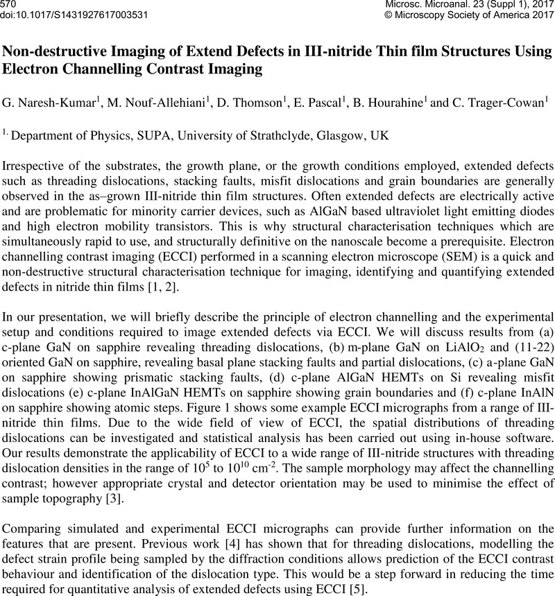
Non-destructive Imaging of Extend Defects in III-nitride Thin film Structures Using Electron Channelling Contrast Imaging
Published online by Cambridge University Press: 04 August 2017
Abstract
An abstract is not available for this content so a preview has been provided. As you have access to this content, a full PDF is available via the ‘Save PDF’ action button.
- Type
- Abstract
- Information
- Microscopy and Microanalysis , Volume 23 , Supplement S1: Proceedings of Microscopy & Microanalysis 2017 , July 2017 , pp. 570 - 571
- Copyright
- © Microscopy Society of America 2017
References
[4]Pascal, E. et al. under review in Materials Today Proceedings (2017).Google Scholar
[5] The authors acknowledge support from the EPSRC, Grant Number EP/M015181/1, “Manufacturing of nano-engineered III-N semiconductors”.Google Scholar
 You have
Access
You have
Access