


No CrossRef data available.
Article contents
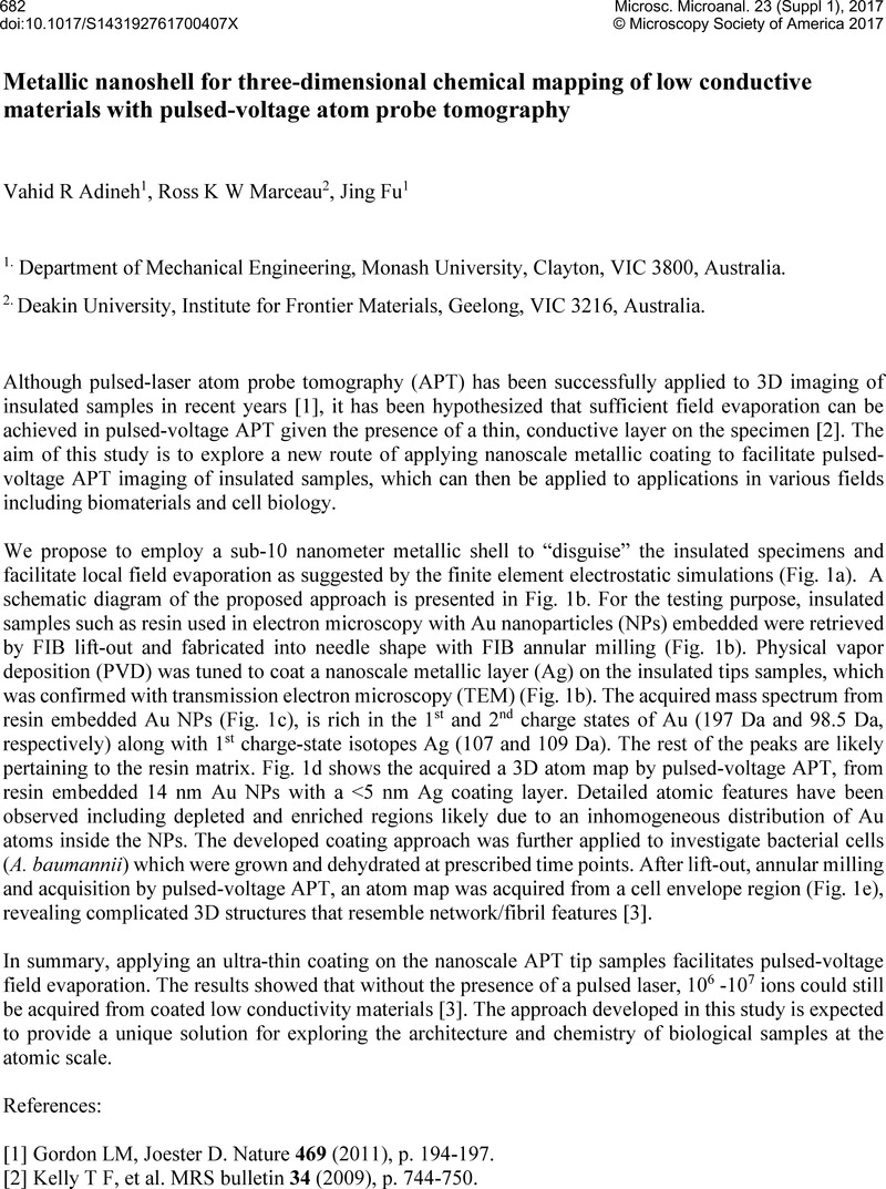
Metallic nanoshell for three-dimensional chemical mapping of low conductive materials with pulsed-voltage atom probe tomography
Published online by Cambridge University Press: 04 August 2017
Abstract
An abstract is not available for this content so a preview has been provided. As you have access to this content, a full PDF is available via the ‘Save PDF’ action button.
- Type
- Abstract
- Information
- Microscopy and Microanalysis , Volume 23 , Supplement S1: Proceedings of Microscopy & Microanalysis 2017 , July 2017 , pp. 682 - 683
- Copyright
- © Microscopy Society of America 2017
References
[4] The authors acknowledge use of facilities within the Monash Centre for Electron Microscopy (MCEM) as well as Institute for Frontier Materials (IFM) - Deakin University. This study was funded by Monash University Interdisciplinary Research (IDR) Seed Fund and the Monash Centre for Atomically Thin Materials (MCATM) for the PhD top-up scholarship.Google Scholar
 You have
Access
You have
Access