Hostname: page-component-7c8c6479df-995ml Total loading time: 0 Render date: 2024-03-28T15:38:17.835Z Has data issue: false hasContentIssue false

Crystallographic Orientation Analysis of Nanocrystalline Tungsten Thin Film Using TEM Precession Electron Diffraction and SEM Transmission Kikuchi Diffraction

Published online by Cambridge University Press:  05 February 2021

Jiwon Jeong
Affiliation:
Department of Energy Science, Sungkyunkwan University (SKKU), Suwon16419, Republic of Korea Max-Planck Institut für Eisenforschung GmbH, Düsseldorf40237, Germany
Woo-Sung Jang
Affiliation:
Department of Energy Science, Sungkyunkwan University (SKKU), Suwon16419, Republic of Korea
Kwang Hun Kim
Affiliation:
Memory Analysis Science & Engineering Group, Samsung Electronics, Hwasung18448, Republic of Korea
Aleksander Kostka
Affiliation:
Zentrum für Grenzflächendominierte Höchstleistungswerkstoffe (ZGH), Ruhr-Universität Bochum, Bochum44801, Germany
Gilho Gu
Affiliation:
Memory Analysis Science & Engineering Group, Samsung Electronics, Hwasung18448, Republic of Korea
Young-Min Kim*
Affiliation:
Department of Energy Science, Sungkyunkwan University (SKKU), Suwon16419, Republic of Korea
Sang Ho Oh*
Affiliation:
Department of Energy Science, Sungkyunkwan University (SKKU), Suwon16419, Republic of Korea
*
*Author for correspondence: Sang Ho Oh, E-mail: sanghooh@skku.edu, Young-Min Kim, E-mail: youngmk@skku.edu
Get access

Abstract

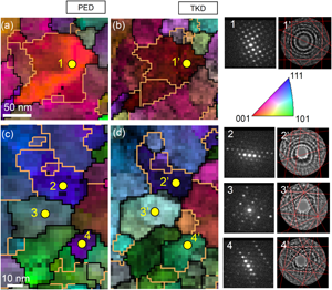
Two advanced, automated crystal orientation mapping techniques suited for nanocrystalline materials—precession electron diffraction (PED) in transmission electron microscopy (TEM) and on-axis transmission Kikuchi diffraction (TKD) in scanning electron microscopy (SEM)—are evaluated by comparing the orientation maps obtained from the identical location on a 30 nm-thick nanocrystalline tungsten (W) thin film. A side-by-side comparison of the orientation maps directly showed that the large-scale orientation features are almost identical. However, there are differences in the fine details, which arise from the fundamentally different nature of the spot pattern and Kikuchi line pattern in terms of the excitation volume and the angular resolution. While TEM-PED is more reliable to characterize grains oriented along low-index zone axes, the high angular resolution of SEM-TKD allows the detection of small misorientation between grains and thus yields better quantification and statistical analysis of grain orientation. Given that both TEM-PED and SEM-TKD orientation mapping techniques are complementary tools for nanocrystalline materials, one can be favorably selected depending on the requirements of the analysis, as they have competitive performance in terms of angular resolution and texture quantification.

Type
Materials Science Applications
Copyright
Copyright © The Author(s), 2021. Published by Cambridge University Press on behalf of the Microscopy Society of America

Access options

Get access to the full version of this content by using one of the access options below. (Log in options will check for institutional or personal access. Content may require purchase if you do not have access.)

Footnotes

a

These authors contributed equally to this work.

References

Abbasi, M, Kim, D-I, Guim, H-U, Hosseini, M, Danesh-Manesh, H & Abbasi, M (2015). Application of transmitted Kikuchi diffraction in studying nano-oxide and ultrafine metallic grains. ACS Nano 9, 1099111002.CrossRefGoogle ScholarPubMed
Brandon, D & Kaplan, WD (2008). Microstructural Characterization of Materials. Hoboken, NJ: Wiley.10.1002/9780470727133CrossRefGoogle Scholar
Brodu, E, Bouzy, E & Fundenberger, J-J (2017). Diffraction contrast dependence on sample thickness and incident energy in on-axis transmission Kikuchi diffraction in SEM. Ultramicroscopy 181, 123133.CrossRefGoogle ScholarPubMed
Cauchois, R, Saadaoui, M, Inal, K, Dubois-Bonvalot, B & Fidalgo, JC (2012). Tailoring the crystallographic texture and electrical properties of inkjet-printed interconnects for use in microelectronics. Mater Res Soc Symp Proc 1335, 119124.Google Scholar
Cooper, D, Bernier, N & Rouvière, JL (2015). Combining 2 nm spatial resolution and 0.02% precision for deformation mapping of semiconductor specimens in a transmission electron microscope by precession electron diffraction. Nano Lett 15, 52895294.CrossRefGoogle Scholar
Cullity, BD & Stock, SR (2001). Elements of X-ray Diffraction, 3rd ed. New York, NY: Prentice Hall.Google Scholar
Dellasega, D, Merlo, G, Conti, C, Bottani, CE & Passoni, M (2012). Nanostructured and amorphous-like tungsten films grown by pulsed laser deposition. J Appl Phys 112, 084328.CrossRefGoogle Scholar
El-Atwani, O, Suslova, A, Novakowski, TJ, Hattar, K, Efe, M, Harilal, SS & Hassanein, A (2015). In-situ TEM/heavy ion irradiation on ultrafine-and nanocrystalline-grained tungsten: Effect of 3 MeV Si, Cu and W ions. Mater Charact 99, 6876.10.1016/j.matchar.2014.11.013CrossRefGoogle Scholar
Fanta, AB, Todeschini, M, Burrows, A, Jansen, H, Damsgaard, CD, Alimadadi, H & Wagner, JB (2018). Elevated temperature transmission Kikuchi diffraction in the SEM. Mater Charact 139, 452462.CrossRefGoogle Scholar
Fundenberger, JJ, Bouzy, E, Goran, D, Guyon, J, Morawiec, A & Yuan, H (2015). Transmission Kikuchi Diffraction (TKD) via a horizontally positioned detector. Microsc Microanal 21(S3), 11011102.10.1017/S1431927615006297CrossRefGoogle Scholar
Fundenberger, JJ, Bouzy, E, Goran, D, Guyon, J, Yuan, H & Morawiec, A (2016). Orientation mapping by transmission-SEM with an on-axis detector. Ultramicroscopy 161, 1722.10.1016/j.ultramic.2015.11.002CrossRefGoogle ScholarPubMed
Garner, A, Gholinia, A, Frankel, P, Gass, M, MacLaren, I & Preuss, M (2014). The microstructure and microtexture of zirconium oxide films studied by transmission electron backscatter diffraction and automated crystal orientation mapping with transmission electron microscopy. Acta Mater 80, 159171.CrossRefGoogle Scholar
Ghamarian, I, Liu, Y, Samimi, P & Collins, PC (2014). Development and application of a novel precession electron diffraction technique to quantify and map deformation structures in highly deformed materials—as applied to ultrafine-grained titanium. Acta Mater 79, 203215.CrossRefGoogle Scholar
Girault, B, Eyidi, D, Goudeau, P, Sauvage, T, Guerin, P, Bourhis, EL & Renault, PO (2013). Controlled nanostructuration of polycrystalline tungsten thin films. J Appl Phys 113, 174310.CrossRefGoogle Scholar
Han, M, Yuan, P, Liu, J, Si, S, Zhao, X, Yue, Y, Wang, X & Xiao, X (2017). Interface energy coupling between β-tungsten nanofilm and few-layered graphene. Sci Rep 7, 12213.CrossRefGoogle ScholarPubMed
Humphreys, FJ (2004). Characterisation of fine-scale microstructures by electron backscatter diffraction (EBSD). Scr Mater 51, 771776.CrossRefGoogle Scholar
Keller, RR & Geiss, RH (2012). Transmission EBSD from 10 nm domains in a scanning electron microscope. J Microsc 245, 245251.CrossRefGoogle Scholar
Langford, RM, Huang, YZ, Lozano-Perez, S, Titchmarsh, JM & Petford-Long, AK (2001). Preparation of site specific transmission electron microscopy plan-view specimens using a focused ion beam system. J Vac Sci Technol A 19, 755758.CrossRefGoogle Scholar
Liu, CM, Lin, HW, Lu, CL & Chen, C (2014). Effect of grain orientations of Cu seed layers on the growth of 〈111〉-oriented nanotwinned Cu. Sci Rep 4, 6123.CrossRefGoogle ScholarPubMed
Liu, J, Lozano-Perez, S, Wilkinson, AJ & Grovenor, CRM (2019). On the depth resolution of transmission Kikuchi diffraction (TKD) analysis. Ultramicroscopy 205, 512.CrossRefGoogle ScholarPubMed
Mayol, R & Salvat, F (1997). Total and transport cross sections for elastic scattering of electrons by atoms. At Data Nucl Data Tables 65, 55154.CrossRefGoogle Scholar
Midgley, PA & Eggeman, AS (2015). Precession electron diffraction—a topical review. IUCrJ 2, 126136.CrossRefGoogle Scholar
Moeck, P, Rouvimov, S, Rauch, EF, Véron, M, Kirmse, H, Häusler, I, Neumann, W, Bultreys, D, Maniette, Y & Nicolopoulos, S (2011). High spatial resolution semi-automatic crystallite orientation and phase mapping of nanocrystals in transmission electron microscopes. Crystallogr Res Technol 46, 589606.10.1002/crat.201000676CrossRefGoogle Scholar
Morawiec, A & Bouzy, E (2006). On the reliability of fully automatic indexing of electron diffraction patterns obtained in a transmission electron microscope. J Appl Crystallogr 39, 101103.CrossRefGoogle Scholar
Morawiec, A, Bouzy, E, Paul, H & Fundenberger, JJ (2014). Orientation precision of TEM-based orientation mapping techniques. Ultramicroscopy 136, 107118.CrossRefGoogle ScholarPubMed
Musil, J, Vlček, J, Ježek, V, Benda, M, Kolega, M & Boomsma, R (1995). Production of Ti films with controlled texture. Surf Coat Technol 76–77, 274279.CrossRefGoogle Scholar
Oleynikov, P, Hovmöller, S & Zou, XD (2007). Precession electron diffraction: Observed and calculated intensities. Ultramicroscopy 107, 523533.CrossRefGoogle ScholarPubMed
Own, CS, Sinkler, W & Marks, LD (2006). Rapid structure determination of a metal oxide from pseudo-kinematical electron diffraction data. Ultramicroscopy 106, 114122.CrossRefGoogle ScholarPubMed
Portillo, J, Rauch, EF, Nicolopoulos, S, Gemmi, M & Bultreys, D (2010). Precession electron diffraction assisted orientation mapping in the transmission electron microscope. Mater Sci Forum 644, 17.CrossRefGoogle Scholar
Rauch, EF & Dupuy, L (2005). Rapid spot diffraction patterns identification through template matching. Arch Metall Maters 50, 8799.Google Scholar
Rauch, EF, Portillo, J, Nicolopoulos, S, Bultreys, D, Rouvimov, S & Moeck, P (2010). Automated nanocrystal orientation and phase mapping in the transmission electron microscope on the basis of precession electron diffraction. Z Kristallogr 225, 103109.CrossRefGoogle Scholar
Rauch, EF & Veron, M (2013). Solving the 180 degree orientation ambiguity related to spot diffraction patterns in transmission electron microscopy. Microsc Microanal 19, 324325.CrossRefGoogle Scholar
Rauch, EF & Véron, M (2014). Automated crystal orientation and phase mapping in TEM. Mater Charact 98, 19.CrossRefGoogle Scholar
Shen, YG, Mai, YW, Zhang, QC, McKenzie, DR, McFall, WD & McBride, WE (2000). Residual stress, microstructure, and structure of tungsten thin films deposited by magnetron sputtering. J Appl Phys 87, 177187.CrossRefGoogle Scholar
Sneddon, G, Trimby, P & Cairney, J (2017). The influence of microscope and specimen parameters on the spatial resolution of transmission Kikuchi diffraction. Microsc Microanal 23, 532533.CrossRefGoogle Scholar
Sneddon, GC, Trimby, PW & Cairney, JM (2016). Transmission Kikuchi diffraction in a scanning electron microscope: A review. Mater Sci Eng R Rep 110, 112.10.1016/j.mser.2016.10.001CrossRefGoogle Scholar
Steinhögl, W, Steinlesberger, G, Perrin, M, Scheinbacher, G, Schindler, G, Traving, M & Engelhardt, M (2005). Tungsten interconnects in the nano-scale regime. Microelectron Eng 82, 266272.CrossRefGoogle Scholar
Thomas, G (1978). Kikuchi electron diffraction and applications. In Diffraction and Imaging Techniques in Material Science, pp. 399427. North-Holland Publishing Company.10.1016/B978-0-444-85128-4.50015-1CrossRefGoogle Scholar
Trimby, PW (2012). Orientation mapping of nanostructured materials using transmission Kikuchi diffraction in the scanning electron microscope. Ultramicroscopy 120, 1624.CrossRefGoogle ScholarPubMed
Trimby, PW, Cao, Y, Chen, Z, Han, S, Hemker, KJ, Lian, J, Liao, X, Rottmann, P, Samudrala, S, Sun, J, Wang, JT, Wheeler, J & Cairney, JM (2014). Characterizing deformed ultrafine-grained and nanocrystalline materials using transmission Kikuchi diffraction in a scanning electron microscope. Acta Mater 62, 6980.CrossRefGoogle Scholar
van Bremen, R, Gomes, DR, de Jeer, LTH, Ocelík, V & De Hosson, JTM (2016). On the optimum resolution of transmission-electron backscattered diffraction (t-EBSD). Ultramicroscopy 160, 256264.CrossRefGoogle Scholar
Viladot, D, Véron, M, Gemmi, M, Peiró, F, Portillo, J, Estradé, S, Mendoza, J, Llorca-Isern, N & Nicolopoulos, S (2013). Orientation and phase mapping in the transmission electron microscope using precession-assisted diffraction spot recognition: State-of-the-art results. J Microsc 252, 2334.CrossRefGoogle ScholarPubMed
Vincent, R & Midgley, PA (1994). Double conical beam-rocking system for measurement of integrated electron diffraction intensities. Ultramicroscopy 53, 271282.10.1016/0304-3991(94)90039-6CrossRefGoogle Scholar
Wollschläger, N, Palasse, L, Häusler, I, Dirscherl, K & Hodoroaba, V-D (2017). Characterization of the inner structure of porous TiO2 nanoparticle films in dye sensitive solar cells (DSSC) by focused ion beam (FIB) tomography and transmission Kikuchi diffraction (TKD) in the scanning electron microscope (SEM). Mater Charact 131, 3948.CrossRefGoogle Scholar
Wright, SI, Nowell, MM & Bingert, JF (2007). A comparison of textures measured using X-ray and electron backscatter diffraction. Metall Mater Trans A 38, 18451855.CrossRefGoogle Scholar
Yuan, H, Brodu, E, Chen, C, Bouzy, E, Fundenberger, J & Toth, LS (2017). On-axis versus off-axis Transmission Kikuchi Diffraction technique: Application to the characterisation of severe plastic deformation-induced ultrafine-grained microstructures. J Microsc 267, 7080.CrossRefGoogle ScholarPubMed
Zaefferer, S (2007). On the formation mechanisms, spatial resolution and intensity of backscatter Kikuchi patterns. Ultramicroscopy 107, 254266.CrossRefGoogle ScholarPubMed
Zaefferer, S (2011). A critical review of orientation microscopy in SEM and TEM. Crystallogr Res Technol 46, 607628.10.1002/crat.201100125CrossRefGoogle Scholar
Supplementary material: File

Jeong et al. supplementary material

Jeong et al. supplementary material

Download Jeong et al. supplementary material(File)
File 8.2 MB