Hostname: page-component-76fb5796d-zzh7m Total loading time: 0 Render date: 2024-04-27T00:56:46.564Z Has data issue: false hasContentIssue false

Beware of Artifacts When Characterizing Nanometer Device Features Smaller than a TEM Lamella Thickness in Semiconductor Wafer-foundries

Published online by Cambridge University Press:  27 August 2014

Wayne Zhao
Affiliation:
Engineering Analysis - Physical, Technology Development & Yield Engineering, Technology Development, GLOBALFOUNDRIES, Malta, New York, USA
Hugh Porter
Affiliation:
Engineering Analysis - Physical, Technology Development & Yield Engineering, Technology Development, GLOBALFOUNDRIES, Malta, New York, USA
Raghaw Rai
Affiliation:
Engineering Analysis - Physical, Technology Development & Yield Engineering, Technology Development, GLOBALFOUNDRIES, Malta, New York, USA
Esther (PY) Chen
Affiliation:
Engineering Analysis - Physical, Technology Development & Yield Engineering, Technology Development, GLOBALFOUNDRIES, Malta, New York, USA
Jeremy Russell
Affiliation:
Engineering Analysis - Physical, Technology Development & Yield Engineering, Technology Development, GLOBALFOUNDRIES, Malta, New York, USA

Abstract

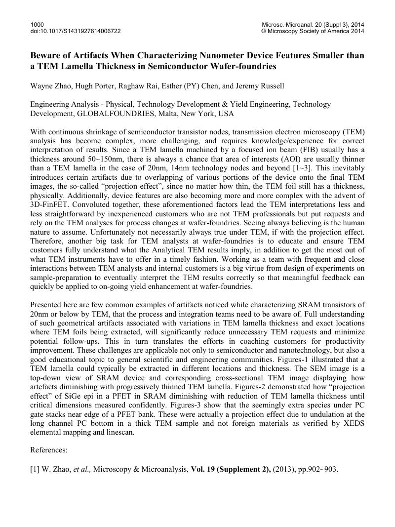
Image of the first page of this content. For PDF version, please use the ‘Save PDF’ preceeding this image.'
Type
Abstract
Copyright
Copyright © Microscopy Society of America 2014 

References

[1] Zhao, W., et al., Microscopy & Microanalysis, Vol. 19(Supplement 2), (2013), pp.902~903.Google Scholar
[2] Zhao, W., et al., Proc. 38th International Symposium for Testing and Failure Analysis (2012), pp. 347~355.Google Scholar
[3] Zhao, W. & Proc, Symp. the Material Research Society, 2002 Fall Meeting (2002), Vol. 738, pp. G7.15.1~6.Google Scholar