


Introduction
X-ray microanalysis is a well-established elemental analysis technique, providing quantified values for the composition of a specimen using either wavelength-dispersive X-ray spectroscopy (WDX) or energy-dispersive X-ray spectroscopy (EDX). Commonly used within geology, metallurgy, and archaeology, both techniques are capable of providing compositional information on a material with a micron-scale measurement volume Goldstein et al. (Reference Goldstein, Newbury, Michael, Ritchie, Scott and Joy2017) coupled with high spatial resolution mapping (Pownceby et al., Reference Pownceby, MacRae and Wilson2007). The very low detection limits possible with WDX also allow the analysis of trace elements (Ritchie et al., Reference Ritchie, Newbury and Davis2012; Batanova et al., Reference Batanova, Sobolev and Magnin2018; Vind et al., Reference Vind, Malfliet, Bonomi, Paiste, Sajó, Blanpain, Tkaczyk, Vassiliadou and Panias2018) with concentrations on the order of 10 ppm (Donovan et al., Reference Donovan, Lowers and Rusk2011) being quantifiable. These same principles have then been applied to semiconductor characterization; using WDX to determine and map the composition of the main semiconductor material and trace element analysis to quantify material dopant densities and identify undesired impurities (Nakajima et al., Reference Nakajima, Yamaguchi, Akita and Kotani1978; Bejtka et al., Reference Bejtka, Edwards, Martin, Fernández-Garrido and Calleja2008; Kusch et al., Reference Kusch, Mehnke, Enslin, Edwards, Wernicke, Kneissl and Martin2017). While there are more established techniques used to determine doping concentrations, such as secondary ion mass spectrometry (SIMS; Chu et al., Reference Chu, Gao and Erickson1998), WDX benefits from being nondestructive and allowing simultaneous acquisition of other characteristic signals such as cathodoluminescence (Lee et al., Reference Lee, Martin, Trager-Cowan and Edwards2005; Pownceby et al., Reference Pownceby, MacRae and Wilson2007; Edwards & Martin, Reference Edwards and Martin2011).
The semiconductor materials under investigation are usually thin layers (100 nm up to several μm) fabricated on polished substrates, which are generally dissimilar. The first step when performing WDX analysis is to analyze the beam penetration depth within the material using Monte Carlo simulations, such as the Casino software (Drouin et al., Reference Drouin, Couture, Joly, Tastet, Aimez and Gauvin2007). As material composition, density and film thicknesses are generally all unknown to some extent, this is just an approximation providing a guide for which beam acceleration voltage to use. Figure 1 shows the results of a Casino simulation of the electron penetration depth within a semiconductor layer on its substrate (Al0.5Ga0.5N/Al2O3) for various beam voltages. In this example, a beam acceleration voltage of 10 kV is low enough to confine the primary excitation within the 600 nm Al0.5Ga0.5N layer. When experimental measurements are performed using the indicated ideal beam conditions, it is assumed that characteristic X-ray generation is contained within the film layer. However, the result could be tainted by the generation of characteristic X-rays by secondary fluorescence from other layers, such as the substrate. If an X-ray with sufficient energy to cause ionization is absorbed by the atoms of the material, it can result in the fluorescence of additional characteristic X-rays. This so-called secondary fluorescence can increase the X-ray counts for the fluorescing element while simultaneously reducing the counts for the element producing the absorbed X-ray (Goldstein et al., Reference Goldstein, Newbury, Michael, Ritchie, Scott and Joy2017).

Fig. 1. Casino simulation of electron penetration depths within an Al0.5Ga0.5N/Al2O3 (ρ = 4.71 g/cm3) semiconductor with a film thickness of 600 nm. Result shown using a beam acceleration voltage of (a) 5 kV, (b) 10 kV, and (c)15 kV.
After the beam of electrons hits a surface, for example in a WDX measurement, a large proportion of the electrons penetrate into the sample where two types of primary X-rays may be produced:
1. Characteristic X-rays with defined energies equal to the energy difference between two electron shells within an atom.
2. Bremsstrahlung X-rays. A continuum of X-rays is produced by the deflection of electrons within the electric field of an atomic nuclei with an energy extending up to the incident beam energy (Goldstein et al., Reference Goldstein, Newbury, Michael, Ritchie, Scott and Joy2017).
Primary X-rays of either type are now capable of producing secondary X-ray fluorescence providing their energy is sufficient to excite further characteristic X-rays. These secondary X-rays are distinguished by their source of excitation: characteristic secondary fluorescence (CSF) and bremsstrahlung secondary fluorescence (BSF). The primary X-rays are excited within the interaction volume of the beam electrons (typically <1 μm in depth, see Fig. 1) but the secondary X-rays can come from much deeper within the sample. The range X-rays can travel in the material is determined by X-ray absorption, which in turn depends on the X-ray energy and matrix atoms and is typically significantly larger than the range of the beam electrons. The rate of absorption of these X-rays within a material is defined by the mass attenuation coefficient (MAC). The MAC of an element is dependent of the energy of the incident X-ray with the highest MAC being at energies just above the absorption edge of a shell. The penetration depth of the secondary excitation volume is dependent on the average MAC of the material, materials with a higher MAC will result in a smaller mean free path of the X-rays and therefore will have a reduced volume compared to materials with a composition featuring lower MACs. The secondary excitation volume due to Ni X-rays in a Ni–Fe alloy is estimated to be 10's of microns (Goldstein et al., Reference Goldstein, Newbury, Michael, Ritchie, Scott and Joy2017). Significantly for WDX measurements, secondary fluorescence is indistinguishable from characteristic primary X-ray emission.
To summarize the basic principle behind X-ray microanalysis: the composition of an unknown material is estimated using ratios (k-ratios) of the number of specific characteristic X-rays emitted from the unknown to that for a standard of known composition. Direct comparisons between the two X-ray counts are insufficient to derive the material composition as corrections must first be applied to the k-ratios to account for various factors that influence the number of X-rays emitted from a specific material. ZAF matrix correction factors are commonly used, with “F” dealing with secondary fluorescence due to the reabsorption of characteristic X-rays within the primary excitation volume, generally treated as a homogeneous bulk material.
These correction factors assume that the unknown material has a homogeneous composition and are therefore unable to account for X-rays generated within an adjacent material of different composition by secondary fluorescence. The primary beam excitation volume may be enclosed within an upper specimen layer but the larger secondary excitation volume may produce CSF and BSF X-rays from the layer beneath. Some of these CSF and BSF X-rays will escape from the specimen and contribute to the X-ray counts. Dalton & Lane (Reference Dalton and Lane1996) showed how secondary fluorescence skews the quantification of olivine minerals as X-rays propagate through neighboring phase boundaries of calcium-rich deposits. Computational papers by Llovet & Galan (Reference Llovet and Galan2003) and Llovet et al. (Reference Llovet, Pinard, Donovan and Salvat2012) showed, using the PENELOPE simulation package, that there is an increase in k-ratio for an indirectly excited metal adjacent to a directly excited metal (a binary material couple) due to secondary fluorescence. DTSA-II (Ritchie, Reference Ritchie2009) was then developed by Ritchie to model secondary fluorescence within EDX experiments in much shorter simulation times and with less computational power than the PENELOPE alternative (Ritchie, Reference Ritchie2017). Despite the reduced calculation time, Ritchie showed that DTSA-II results successfully matched that of Llovet, both packages being in agreement with experimental work performed by Bastin et al. (Reference Bastin, van Loo, Vosters and Vrolljk1983). X-ray generation within film–substrate materials is well established within the literature including the impact of secondary fluorescence. Pouchou & Pichoir (Reference Pouchou, Pichoir, Heinrich and Newbury1991) noted the issues that may occur when performing X-ray microanalysis on thin heavy-metal films with substrate secondary fluorescence contributing nearly 10% of the total X-rays generated. Pouchou (Reference Pouchou2002) then went on to quantify the impact secondary fluorescence could have within a metal–metal system noting that secondary fluorescence could produce an unrecognizable error when performing quantitative measurements on these materials. The same behavior was also demonstrated through simulation by Yuan et al. (Reference Yuan, Demers, Rudinsky and Gauvin2019), as well as for a directly excited element embedded within an indirectly excited surrounding material (Yuan et al., Reference Yuan, Demers, Wang and Gauvin2020). Further correlation of experimental and computation work was undertaken by Fournelle et al. (Reference Fournelle, Kim and Perepezko2005) by comparing experimental results of the secondary fluorescence of Nb through phase boundaries with PENELOPE simulations, finding a strong agreement between the two. Recent studies have now developed software for thin-film X-ray microanalysis capable of calculating the extent of secondary fluorescence within the measurements while accurately determining film thicknesses and composition (Moy & Fournelle, Reference Moy and Fournelle2021).
Figure 2 shows compositions resulting from DTSA-II simulations of measurements in metal bilayers which are known to be susceptible to secondary fluorescence (Bastin et al., Reference Bastin, van Loo, Vosters and Vrolljk1983; Yuan et al., Reference Yuan, Demers, Wang and Gauvin2020). All of the examples in Figure 2 consist of a pure copper film of various thicknesses upon a transition metal substrate; nickel, cobalt, and iron. WDX analyses were simulated for these materials (using the method described below) with a beam acceleration voltage of 10 kV to entirely contain the primary excitation volume within the copper layer in all cases. The composition returned by the WDX analysis should be 100% Cu with no Ni, Co, or Fe but secondary fluorescence is seen to produce a “false” presence of the substrate metal within the film composition. In some of these cases, secondary fluorescence has skewed the quantification by greater than 5 at%. For semiconductor thin films, it is not uncommon for an element to be present in both the film and the substrate (e.g., Al in AlxGa1−xN/Al2O3 or AlxGa1−xN/AlN). If the Al quantification was skewed by secondary fluorescence from Al in the substrate, then this could be a significant issue, leading us to draw incorrect conclusions about the material's properties based on this false quantification. It is thus important to understand the impact of secondary fluorescence on WDX analysis of our structures in order to quantify how much the results are affected by secondary fluorescence and to develop approaches to correct for this undesired effect.

Fig. 2. DTSA-II simulation results showing the effect of secondary fluorescence on the quantification of a Cu film with three different transition metal substrates (Ni, Co, and Fe). Cu–Ni (Cu) corresponding to the quantified value of Cu within the Cu film–Ni substrate system.
The structures of many semiconductor devices such as LEDs, solar cells, and advanced transistors, such as high-electron mobility transistors (HEMTs), consist of multiple layers of different semiconductor materials. Specifically within the active region of UV LEDs, there may be a multi-quantum well (MQW) active region composed of multiple layers of AlxGa1−xN, with higher levels of AlN pushing the emission deeper into the UV (Mehnke et al., Reference Mehnke, Sulmoni, Guttmann, Wernicke and Kneissl2019; Amano et al., Reference Amano, Collazo, De Santi, Einfeldt, Funato, Glaab, Hagedorn, Hirano, Hirayama, Ishii, Kashima, Kawakami, Kirste, Kneissl, Martin, Mehnke, Meneghini, Ougazzaden, Parbrook, Rajan, Reddy, Römer, Ruschel, Sarkar, Scholz, Schowalter, Shields, Sitar, Sulmoni, Wang, Wernicke, Weyers, Witzigmann, Wu, Wunderer and Zhang2020). Similar MQW layers composed of InxGa1−xN are found within the blue LEDs that pioneered the transition from incandescent light to solid state lighting over recent years (Akasaki, Reference Akasaki2007). HEMTs used within high power electronics are generally composed of a layered structure containing a high bandgap material such as InxAl1−xN or AlxGa1−xN on top of a lower bandgap material such as GaN (Turuvekere et al., Reference Turuvekere, Karumuri, Rahman, Bhattacharya, Dasgupta and Dasgupta2013). The active layer thicknesses within these structures are often on the order of a few nanometers, making them difficult to measure using X-ray microanalysis. Therefore, prior to device design and manufacture, the materials are generally characterized in thicker layers. These samples consist of much thicker layers (100 s to 1,000 s nm) more suited for determination of elemental composition by X-ray analysis (Martin et al., Reference Martin, Edwards, O'Donnell, Mackay and Watson2002; Bejtka et al., Reference Bejtka, Edwards, Martin, Fernández-Garrido and Calleja2008; Foronda et al., Reference Foronda, Hunter, Pietsch, Sulmoni, Muhin, Graupeter, Susilo, Schilling, Enslin, Irmscher, Martin, Wernicke and Kneissl2020).
The III-nitride semiconductor family covers materials from AlN, emitting in the deep ultraviolet (UV-C), to InN, emitting in the infrared. This opens the way to tertiary and quaternary alloys covering an extremely large range of bandgaps and with high breakdown voltages, making them very desirable for use within optoelectronic devices and high-power electronics. Due to the increasing importance of Al-containing semiconductors for these devices, it is now essential to be able to accurately measure the Al composition within these materials, especially when grown on substrates also containing Al. The bandgap of AlxGa1−xN alloys can be tuned to emit in a specific region of the UV by controlling the composition of the material, with x being equal to the molar fraction of AlN (or Al cation fraction) in the material (Nepal et al., Reference Nepal, Li, Nakarmi, Lin and Jiang2005). The optical properties of a material can therefore be tailored once a reliable growth method is established. WDX has previously been used to characterize AlxGa1−xN (Foronda et al., Reference Foronda, Hunter, Pietsch, Sulmoni, Muhin, Graupeter, Susilo, Schilling, Enslin, Irmscher, Martin, Wernicke and Kneissl2020; Spasevski et al., Reference Spasevski, Kusch, Pampili, Zubialevich, Dinh, Bruckbauer, Edwards, Parbrook and Martin2021); however, it is unknown to what degree secondary fluorescence may have had an impact on these results. Another important III-nitride alloy is InxAl1−xN, which is usually grown on GaN substrates for low InN fractions. A particularly important InN molar percent is 18%, since GaN and the alloy are lattice-matched at this point (Lorenz et al., Reference Lorenz, Franco, Alves, Watson, Martin and O'Donnell2006). Lattice-matched alloys are typically used for power electronics within high frequency, high-electron mobility transistors (HEMTs) (Kuzmík et al., Reference Kuzmík, Kostopoulos, Konstantinidis, Carlin, Georgakilas and Pogany2006), near-UV LED devices (Pampili et al., Reference Pampili, Zubialevich, Maaskant, Akhter, Corbett and Parbrook2019), and integrated within III-nitride LEDs to improve efficiency issues within the green wavelength range (Choi et al., Reference Choi, Kim, Kim, Liu, Kim, Ryou, Dupuis, Fischer and Ponce2010). While applications primarily use near-lattice-matched alloys, InxAl1−xN alloys have been grown for higher InN concentrations with the material bandgap ranging from the infrared to UV-C (Schulz et al., Reference Schulz, Caro, Tan, Parbrook, Martin and O'Reilly2013; Dinh et al., Reference Dinh, Hu, Honda, Amano and Pristovsek2020). WDX measurements have previously been used to quantify the composition of InxAl1−xN on GaN bilayers (Amabile et al., Reference Amabile, Martin, Wang, Whitehead and Parbrook2003; Taylor et al., Reference Taylor, Smith, Sadler, Lorenz, Li, Alves, Parbrook and Martin2014) and have identified high levels (>10%) of unexpected Ga incorporation within the InxAl1−xN (Taylor et al., Reference Taylor, Smith, Sadler, Lorenz, Li, Alves, Parbrook and Martin2014). This was attributed to residual Ga within the growth reactor, left behind from the growth of previous Ga-containing layers, but it is important to clarify whether any of the measured Ga originated from secondary fluorescence during the WDX analysis.
Note that the III-nitride semiconductor alloys follow a strict stoichiometry, with the amount of nitrogen fixed at 50 at% in good quality material. Thus, for tertiary and quaternary alloys, the composition is described in terms of the molar percentages of binary nitride materials rather than the individual elements. For example, within AlxGa1−xN, the composition is described by the molar percentages of AlN and GaN, being x and 1−x, respectively. This stoichiometry rule is used as an indication of a successful WDX analysis, in addition to the check on the overall total wt%. The measured atomic fraction of N should be very close to 50%. It is usually the ratio of group III elements, such as Al and Ga, that is important and to remove any impact of small deviations of the N at% from 50%, the ratio of Al to the total Al + Ga at% is used to give “x” in AlxGa1−xN, and thus the molar percentages of AlN and GaN. This approach is used in the following results sections, investigating how secondary fluorescence influences the determination of the alloy composition.
The aim of this study is to investigate the influence of secondary X-ray fluorescence on the calculated composition of semiconductor materials, quantifying the contributions of CSF and BSF. The DTSA-II Monte Carlo X-ray simulation program was used to perform computational EDX/WDX measurements on various film–substrate semiconductor material combinations. The CalcZAF (Probe Software, Inc.) X-ray quantification program (Armstrong et al., Reference Armstrong, Donovan and Carpenter2013) was used to calculate the k-ratios and material compositions from the X-ray counts produced by DTSA-II. The published studies mentioned above typically use a high beam voltage (e.g., 30 kV); however, we restrict this to a smaller value (10 kV apart from within beam voltage dependence investigations), as this is typical of that used for experimental characterization of semiconductor thin films. Semiconductor film thicknesses for the materials studied in this investigation (III-nitrides, gallium oxide compounds) are typically <1 μm, meaning that such a beam voltage is the highest that can contain the primary excitation volume within the semiconductor film (see Fig. 1) while producing a sufficiently high overvoltage to excite at least one characteristic X-ray transitions for each element.
Materials and Methods
DTSA-II was used to simulate electron beam-induced X-ray generation within three wideband gap semiconductor films on their typical substrates:
1. AlxGa1−xN on substrates of GaN and AlN (Kusch et al., Reference Kusch, Mehnke, Enslin, Edwards, Wernicke, Kneissl and Martin2017),
2. InxAl1−xN on a GaN substrate (Kuzmík et al., Reference Kuzmík, Kostopoulos, Konstantinidis, Carlin, Georgakilas and Pogany2006), and
3. SnGaO on a silicon substrate (Hatipoglu et al., Reference Hatipoglu, Hunter, Mukhopadhyay, Williams, Edwards, Martin, Schoenfeld and Naresh-Kumar2021).
The raw X-ray counts were then converted into k-ratios to give a value for the material composition. For each DTSA-II simulation, there were three compositions generated:
1. A composition using only the primary characteristic X-rays.
 $$k = \displaystyle{{I_{{\rm unk}}( {{\rm Char}} ) } \over {I_{{\rm std}}( {{\rm Char}} ) }}.$$
2. A combination of the primary characteristic X-rays and any X-rays produced through CSF.
$$k = \displaystyle{{I_{{\rm unk}}( {{\rm Char} + {\rm CSF}} ) } \over {I_{{\rm std}}( {{\rm Char} + {\rm CSF}} ) }}.$$3. The total X-ray counts from all generation methods (primary fluorescence, CSFs, and BSFs).
$$k = \displaystyle{{I_{{\rm unk}}( {{\rm Char} + {\rm CSF} + {\rm BSF}} ) } \over {I_{{\rm std}}( {{\rm Char} + {\rm CSF} + {\rm BSF}} ) }}.$$


which is the one that would be used in standard WDX measurements.
In the cases where the atomic composition was calculated the k-ratios were submitted into CalcZAF to generate a quantification of the sample layer. ZAF corrections were calculated using the Love-Scott II package in CalcZAF with the Reed/Armstrong option for F correction.
Example X-ray spectra produced by DTSA-II are shown in Figure 3.

Fig. 3. Example X-ray spectra produced by DTSA-II for various semiconductor materials.
DTSA-II generates a broad peak X-ray spectrum from each simulation comparable to an EDX spectrum; however, it is the underlying raw X-ray counts for specific X-ray lines that are used within the quantification. For each simulation, a beam acceleration voltage of 10 kV and a probe dose (current × time) of 400 nAs were used. This provided a high enough beam energy to excite the desired X-rays for each element and generated a sufficient X-ray peak-background signal to allow reliable quantification. Multiple electron trajectories were applied within DTSA-II to reduce the randomness between simulations. For each film thickness and composition, 16 simulations were completed, compiled, and averaged to produce the average X-ray counts which were used to calculate the k-ratios, which may be submitted into CalcZAF to produce the material quantification. This allowed us to be confident that randomness was not interfering with our results. For each alloy, simulations were run with a range of film thicknesses, increasing in increments of 100 nm to cover material thicknesses up to and beyond the point at which incident electrons penetrate the top layer. For all investigations in this publication, the smallest film thickness simulated is the minimum one required to prevent the primary excitation penetrating into the second layer (for the lower density cases in a series, such as Al0.7Ga0.3N, there may be a small amount of penetration at the lowest thickness). This allows analysis of how the impact of secondary fluorescence changes as the primary excitation volume approaches the film-underlayer boundary. Each simulation took 30–45 min using a personal computer featuring a 2.3 GHz Intel Core i5 processor, 8 GB RAM.
CalcZAF was used to calculate the material quantification from the X-ray counts produced by DTSA-II due to the greater precision (not accuracy) obtainable in the outputted quantification than for the integrated quantification tool within DTSA-II. For each simulation, the material composition was first determined with consideration of only primary X-ray generation and the resulting base composition was then subtracted from subsequent quantifications featuring secondary X-ray generation (CSF and/or BSF) to derive the effect that secondary fluorescence has on the elemental atomic fractions (at%). Simulation results are presented either as unnormalized changes to the elemental k-ratios or as the difference in the atomic or molar fractions. During the calculation of the at% from the elemental k-ratios, the ZAF corrections are applied and the compositions are normalized to 100% to present the semiconductor compound composition in its standard form. When calculating the impact of secondary fluorescence, this normalization process can have a significant impact, for example producing a negative change for an element whose X-ray counts show little/zero change as a result of increased X-ray counts for a different element. We, therefore, present the results in two forms, the difference in k-ratios when explaining the impact of the individual secondary fluorescence effects (CSF and BSF) and changes in atomic percent or molar fraction to explain the impact on the compound composition from secondary fluorescence. The following standards and X-ray lines were used for all quantifications: AlN for Al Kα and N Kα; GaN for Ga Lα; InP for In Lα; silicon for Si Lα; and cassiterite (SnO2) for Sn Lα and O Kα X-rays.
Results and Discussion
AlxGa1−xN
The influence of secondary fluorescence on the elemental atomic fractions quantified by WDX was investigated for a series of AlxGa1−xN films deposited on both GaN and AlN substrates. Two AlxGa1−xN alloys were investigated, with x = 0.3 and 0.7. The excitation volume is estimated to just reach the film–substrate boundary when the film thickness is 600 and 700 nm for x = 0.3 and 0.7, respectively. Figure 4 shows the impact of including secondary fluorescence within the material quantification. Positive (negative) numbers on the vertical axis indicate an increase (decrease) in the k-ratio of an element in the film.

Fig. 4. The change in k-ratio for Ga and Al due to secondary fluorescence mechanisms. Specifically, the effect of CSF for (a) Ga and (b) Al and the effect of BSF on (c) Ga and (d) Al. Two AlxGa1−xN alloys are shown in each figure where x = 0.3 (ρ = 5.28 g/cm3) and 0.7 (ρ = 4.13 g/cm3).
Consider first the impact of CSF on the Ga and Al contents, for which results are plotted in Figures 4a and 4b. For a beam voltage of 10 kV, the Al K absorption edge has the highest energy in the AlxGa1−xN material system. Thus, no additional Al Kα X-rays are produced by CSF [for a beam voltage of 10 kV, it is possible to generate Ga Kα X-rays (E = 9.2 keV), meaning that it is theoretically possible to generate Al Kα X-rays through CSF, however the probability of generating Ga Kα X-rays and subsequent Al Kα CSFs is so low that the counts generated through this process are negligible]. On the other hand, additional Ga Lα X-rays can be excited by CSF by the higher energy Al Kα X-rays and there is a small increase in the Ga X-ray counts. The effect of including CSF within the k-ratio calculation is shown in Figures 4a and 4b. Increasing the AlN molar fraction (x) in the film results in more CSF of Ga Lα X-rays and increases the magnitude of the changes, reaching a maximum increase in k-ratio of approximately 1.4 × 10⁻³ as seen by the red circles and rings in Figure 4a. As there are no additional Al Kα X-rays generated through CSF, the changes for this process are 0 for all film compositions and substrates.
The primary excitation volume is entirely enclosed within the AlxGa1−xN layer, but the secondary excitation volume extends into the substrate and will excite additional Ga X-rays by CSF when the substrate contains Ga. As the AlN molar fraction is increased within the film, there is a steep reduction in film density, pushing the primary excitation volume closer to the substrate and resulting in more Ga secondary fluorescence. Increasing the film layer thickness reduces the magnitude of the difference between substrate materials by containing more of the secondary excitation volume in the film layer, reducing the number of substrate X-rays being generated (and emitted) and causing results from the two substrates to converge.
The impact of BSF on the Ga and Al contents is shown in Figures 4c and 4d. BSF causes a greater increase in Ga or Al at% when that element is present within the substrate as Al Kα X-rays may now also be generated by BSF by the high energy bremsstrahlung, increasing the Al X-rays counts which were previously unchanged by CSF.
The magnitude of the changes induced by BSF are much smaller for Ga than that of CSF seen in Figure 4c. The mass attenuation coefficient of Ga is always greater than that of Al within the 0–10 keV energy range, with the largest differences being in the energy range between the Ga L X-ray and Al K X-ray absorption edges (E = 1.29 and 1.56 keV, respectively). As a result, BSF has a much greater effect on Ga than Al, as seen in Figures 4c and 4d. It should be noted that as our simulations are featuring the Ga L X-ray transitions, there will be a reduced fluorescence yield compared to K transitions (Miller, Reference Miller, Reilly, Ensslin, Smith and Kreiner1991). Knowing this, we would expect BSF to have a greater impact on Al than Ga; however, the superior MAC of Ga prevents this. As the Ga MAC is very large at the Al Kα X-ray energy, there is a large degree of X-ray reabsorption preventing the emission of the Al X-rays, reducing the impact BSF has on the Al k-ratio. Increasing the film thickness reduces the number of substrate BSF X-rays escaping the sample and the change in at% for the two substrates converge to a single value for the thickest films, where substrate BSFs no longer influence the material composition. Increasing x increases the material density, reducing the primary excitation volume and the subsequent secondary fluorescence volume resulting in fewer substrate origin X-rays similarly to CSF.
The previously shown results are in terms of k-ratio, which masks the changes in nitride molar fraction, as is conventionally used to describe the composition of the semiconductor compound (e.g., AlxGa1−xN). We now look at the total effect secondary fluorescence has on the quantified nitride molar fraction. The combined effect of CSF and BSF is shown in Figure 5 for GaN and AlN, respectively. As stated earlier, it is now assumed that the nitrogen content within the material is equal to 50% and we record the material composition as the molar percentages of AlN and GaN. As there are only two materials to be considered within the quantification, any changes experienced by one (e.g., GaN) will result in an equal but opposite change for the other (AlN). The changes are mirrored versions of each other with the change in GaN molar fraction being shown on the left axis and AlN on the right axis. The overall change observed within the GaN molar percent is a slight increase, <0.1%, for all alloy compositions, approximately 0.07% for the high AlN content alloy (x = 0.7) and 0.03% for the low AlN alloy (x = 0.3). The increased value for GaN is dominated by the increase produced from CSF, which is why the largest change is observed for x = 0.7 with the largest number of Al atoms to act as sources for CSF.

Fig. 5. The change in molar fraction for GaN (left axis) and AlN (right axis) due to the combined effect of CSF + BSF. Two AlxGa1−xN alloys are shown in each figure where x = 0.3 (ρ = 5.28 g/cm3) and 0.7 (ρ = 4.13 g/cm3).
The non-zero convergence points for the results from the two substrates at large thicknesses are due to secondary fluorescence in the upper layer, which is normally largely corrected for by “F” in ZAF (although BSF is not included in the calculation for F). Once CSF was removed from the quantification, the contribution of this fluorescence is no longer included in the X-ray counts but the correction factor remains within the calculation of composition. The higher convergence point for Ga when x = 0.7, compared to that for 0.3, is due to the increased Al content resulting in greater excitation, and reduced reabsorption, of Ga CSF. This is in accordance with the Ga “F” factor, which gives a larger reduction factor of 0.9906 for x = 0.7 compared to 0.9930 for x = 0.3 (“F” = 1 in the case of zero secondary fluorescence). In the case of Al (Fig. 1b), there is no contribution from CSF but the results are offset from zero due to the Al compensating the increase to Ga during the normalization of the X-ray counts to elemental fractions (Ga + Al + N = 100 wt%) as mentioned previously.
Knowing that secondary fluorescence produces a low magnitude change in our calculation of the material composition, we can now be confident that previous results are unaffected by these effects. The variation in the results from secondary fluorescence would be contained within the experimental uncertainty and would not need to be specifically addressed for WDX measurements on AlxGa1−xN materials.
InxAl1−xN/GaN
Next, we investigate the impact of secondary fluorescence on WDX data measured from a thin layer of InxAl1−xN on a thick GaN underlayer. The presence of indium within the film is of interest when considering secondary fluorescence due to the high energy primary characteristic X-ray (In Lα 1 at 3.287 keV) which will result in a large CSF excitation volume. The greater MAC for In for higher energy X-rays will also influence how SF impacts the measured compositions. Taylor et al. (Reference Taylor, Smith, Sadler, Lorenz, Li, Alves, Parbrook and Martin2014) reported the unexpected incorporation of gallium in films of InxAl1−xN using WDX. The source of the gallium impurity was determined to be contamination from the growth chamber; however, secondary fluorescence from substrate gallium could have augmented the quantified concentration of gallium impurities within the film, and it is therefore important to verify the source of these unexpected X-rays.
Figure 6 shows the effect of CSF on the k-ratio for all elements present in the material system. For this material, CSF shows different behavior to that for AlxGa1−xN with the element with the highest energy X-ray, In, acting as a source of CSF as well as generating additional In CSF X-rays. This is due to the In Lα 1 X-ray being excited through CSF by higher energy In L transition X-rays (e.g., Lɣ1). The number of these X-rays produced is small but still results in a small increase in the In k-ratio as the film thickness is increased, as seen by the green inverted triangles in Figure 6. The initial negative magnitude of the effect of CSF on In (and N) is due to differences in X-ray generation rates between the standard and film which would be corrected for by the ZAF factors once the k-ratio is quantified.

Fig. 6. The change in k-ratio under the influence of CSF for Al, Ga, In, and N for three InxAl1−xN/GaN alloys where x = 0.1 (ρ = 3.62 g/cm3), 0.2 (ρ = 3.97 g/cm3), and 0.3 (ρ = 4.33 g/cm3).
The blue triangles in Figure 6 show that there is now the apparent presence of Ga within the material with the Ga Lα X-rays being generated by CSF from Al and In X-rays. As the film thickness is increased the amount of “false” Ga is reduced as the Ga X-rays from the substrate have to travel further to the surface, increasing the chance of reabsorption. As x is increased, the increase in material density and the substitution of Al with higher MAC In also suppresses the number of Ga X-rays being emitted, further reducing the change in k-ratio. The red circles in Figure 6 show the Al k-ratio increases when CSF is included with additional Al Kα X-rays being generated by the high energy In X-rays. As x is increased to 0.2, the increase in the Al k-ratio is emphasized as more In sources of CSF excitation are introduced in the film. Further increase of x then begins to reduce the Al k-ratio as the greater In content begins to enhance X-ray reabsorption. The low MAC for N and high rate of N Kα X-ray reabsorption by the other present elements results in an insignificant change in the N X-ray counts, the black squares in Figure 6, with the reduction in k-ratio being attributed to the uncorrected X-ray generation issues mentioned above.
The effect of including BSF within the quantification is now considered in Figure 7. As with CSF, there is now the presence of “false” Ga produced from BSF excitation of the GaN substrate, seen by the blue triangles in Figure 7. Similarly to CSF, as x is increased the number of emitted BSF Ga X-rays quickly decreases and the k-ratio reverts to zero. For N (black squares in Fig. 7), there is little change when BSF is included in k-ratio calculations and no change is seen as the film thickness is increased. As x is increased, there is a small increase in the N k-ratio as the increased In concentration results in the generation of more bremsstrahlung continuum X-rays, allowing N to produce a small additional number of BSF X-rays. Similarly to CSF, the k-ratio for In is initially reduced when BSF X-rays are included with this behavior, now extending to Al as well (green inverted triangles and red circles in Fig. 7 respectively). As the film thickness is increased more of the BSF excitation volume is enclosed within the film, increasing the number of Al and In BSF X-rays generated therefore increasing the k-ratio. As x is increased, the In k-ratio begins to massively increase, dominating continuum absorption with the superior MAC compared to Al, reaching a maximum k-ratio increase of approx. 1.2 × 10⁻³ at the largest film thicknesses. The Al k-ratio continues to increase as x increases but the effect of increasing the film thickness is suppressed for the high In content films. Again the increased In content in the films will result in the generation of a greater number of continuum X-rays, helping to magnify the behavior seen when x = 0.1 but the emission of Al BSF X-rays will be negated by the superior MAC of In.

Fig. 7. The change in k-ratio under the influence of BSF for Al, Ga, In, and N for three InxAl1−xN/GaN alloys where x = 0.1 (ρ = 3.62 g/cm3), 0.2 (ρ = 3.97 g/cm3), and 0.3 (ρ = 4.33 g/cm3).
The combined effect of both secondary fluorescence mechanisms on the molar percentages of the three III-N materials present with the alloys is shown in Figure 8. When the atomic percentages are converted to nitride molar fractions, there is no change in N. An increase in molar fraction is observed for InN and GaN mirroring the overall increase in k-ratio, however the AlN must now decrease to compensate for the increase in the other molar percentages. As the InN content within the alloy is increased the amount of substrate GaN (red markers) detected decreases as the increased number of high MAC In atoms prevents more X-rays reaching the substrate and decreases the chance of Ga secondary fluorescence X-rays being emitted from the sample. The amount of GaN calculated to be within the material with a 1 μm film thickness as a result of secondary fluorescence is found to be approximately 0.018% when x = 0.1, further decreasing to 0.01% and 0.003% when x = 0.2 and 0.3, respectively. This confirms that when large amounts of GaN are unexpectedly detected, as in Taylor et al. (Reference Taylor, Smith, Sadler, Lorenz, Li, Alves, Parbrook and Martin2014), that the cause is likely to be due to material impurities rather than secondary fluorescence.

Fig. 8. Effect of secondary fluorescence on the molar fraction of GaN, InN, and AlN for three InxAl1−xN/GaN alloys where x = 0.1 (ρ = 3.62 g/cm3), 0.2 (ρ = 3.97 g/cm3), and 0.3 (ρ = 4.33 g/cm3).
As expected, when the InN content increases within the alloy the increase in the reported molar percent due to secondary fluorescence for InN (blue markers) increases, as there are more In atoms present. For x = 0.1, the increase in molar percent for InN is 0.012% and the decrease in AlN is −0.03% for a 1 μm film. For x = 0.2 and 0.3, the increase in InN grows to approximately 0.022% and 0.035%, respectively. When x = 0.1, the AlN change (black markers) is compensating for the increase in both GaN and InN, but as the InN content in the alloy increases the number of Ga X-rays abruptly decreases and the AlN begins to compensate for just the increase in InN, explaining the change in trend for AlN for thinner film thicknesses. Again, the change in AlN is small, with decreases of approximately −0.032% and −0.039% for x = 0.2 and 0.3, respectively. As with the elemental changes, the magnitude of all the changes to the molar percent for the three III-nitride binary materials sums to 0.
As with the previous AlxGa1−xN study, the magnitude of the change is minimal and well within the uncertainty margins if measured experimentally. We can therefore be confident of our results when experimentally characterizing these materials. For III-nitride materials, the effect of secondary fluorescence within the material is by no means great enough to produce a large change in the quantification of the material when operating at a beam voltage of 10 kV. When performing compositional analyses on a film within a film–substrate material then substrate X-rays interfering with the material quantification have also been found to be negligible under the same conditions; however, it is unknown if results could be skewed if one was using WDX to perform trace element analyses or determining dopant densities within the material.
(SnxGa1−x)2O3
Gallium oxide (Ga2O3) is an emerging ultra-wide bandgap semiconductor with a bandgap of E g = 4.6–4.9 eV depending on the material polymorph and/or the polarization (Pearton et al., Reference Pearton, Yang, Cary, Ren, Kim, Tadjer and Mastro2018). This semiconductor and its ternary alloys are currently the focus of intensive research for use in UV devices and high power transistors (Hatipoglu et al., Reference Hatipoglu, Mukhopadhyay, Alema, Sakthivel, Seal, Osinsky and Schoenfeld2020). Tin is a commonly used dopant with Ga2O3, providing n-type conductivity to enable use in solar-blind UV photodetectors (Xu et al., Reference Xu, Zheng and Huang2019). Recent publications (Mukhopadhyay & Schoenfeld, Reference Mukhopadhyay and Schoenfeld2019) have also shown that alloying with larger amounts of tin significantly improves the performance of the photodetectors as well as inducing a shift in the material band gap. This bandgap shift can be up to −0.4 eV with low concentrations of tin within the alloy (Sn ≃ 10%), so precise knowledge of the material composition is required to determine the optical properties (Mukhopadhyay & Schoenfeld, Reference Mukhopadhyay and Schoenfeld2020). Here, we have performed simulations, based on experimental WDX results, on (SnxGa1−x)2O3 samples with increasing fractions of tin oxide to assess the influence of secondary fluorescence on the material composition.
Two different types of tin–gallium oxide (SnxGa1−x)2O3 sample were measured using WDX:
1. Films grown directly onto a silicon substrate (SnxGa1−x)2O3/Si and
2. Films grown on a Ga2O3 buffer layer upon a silicon substrate (SnxGa1−x)2O3/Ga2O3/Si.
With film thicknesses of approximately 300 nm, experimental measurements had to be performed at 6 kV, with a 40 nA beam current, to keep the primary excitation within the top layer, although this energy is nonideal for efficiently generating the Sn Lα X-rays (E = 3.444 keV). The experimental results determined that a sample of (SnxGa1−x)2O3 had atomic fractions of approximately 60% O, 38% Ga, and 2% Sn. This composition was then used as the basis for the (SnxGa1−x)2O3 composition in the DTSA-II simulations. It is expected that the Sn would replace Ga in Ga2O3. Although the possible formation of the tin oxide polymorph SnO2 means that the elemental atomic fractions may deviate from the 2:3 metal:oxygen ratio. We will therefore discuss the Sn concentration in terms of atomic percent, at% and refer to tin–gallium oxide as TGO going forward. The relative gallium and tin concentrations were then varied from Sn = 1 at% to 4 at%. As we have established the individual effects of CSF and BSF on the material k-ratio, we will now only present the results as the total effect secondary fluorescence has on the elemental at%.
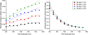
As the previous studies established that secondary fluorescence has a minimal effect on our compositional measurements of the major elemental constituents in semiconductor alloys, we have now focused on the low concentration element of tin and the substrate silicon. The apparent change in at% for tin and silicon are plotted in Figure 9, for four different layer compositions (Sn at% = 1–4 at%). Again, the overall magnitude of the secondary fluorescence contribution is very low, with a <0.1 at% difference being observed for both the film Sn, Figure 9a, and the substrate Si, Figure 9b. Figure 9a shows that the secondary fluorescence mechanisms result in the marginal increase in the Sn at% coming exclusively from BSF due to Sn Lα being the highest energy X-ray in the system. (As with In Lα in the previous example, there is CSF of Sn Lα X-rays generated by higher energy L-shell Sn X-rays but the number of these events is so low as to have a negligible impact.) The high Sn MAC results in an increase in bremsstrahlung absorption as the Sn concentration is increased resulting in a larger increase in the Sn at%, similarly to indium in the previous example. Figure 9b shows the amount of “false” silicon that has been included in the material quantification due to X-rays originating from secondary fluorescence in the substrate. The Si K absorption edge has an energy of E = 1.84 keV, so excitation of the Kα X-ray line is by either BSF or by CSF generated by Sn Lα X-rays, with increasing concentrations of Sn generating more Si X-rays by CSF. As before, increasing the film thickness contains the secondary excitation volume within the upper layer reducing the number of Si X-rays generated.

Fig. 9. The change in atomic fraction under the influence of secondary fluorescence for (a) tin and (b) silicon. The results from four alloys are shown where Sn at% is varied from 1 to 4%.
While this secondary volume has little effect on the quantification of the bulk material, it would become significant when analyzing dopants within the film. Silicon is another commonly used n-type dopant within Ga2O3 (Zhang et al., Reference Zhang, Arita, Wang, Chen, Saito, Tanaka, Nishio, Motooka and Guo2016) which can be measured through WDX. If the silicon-doped semiconductor film were grown on a silicon substrate, then secondary fluorescence would contribute to an incorrect concentration of dopants. For example, a 1 μm film with Sn = 2 at% produced a quantified atomic value for Si = 0.016 at% which translates to a Si dopant density on the order of 1018 atoms cm−3. A study on how this “false” concentration of Si could be reduced was then conducted by investigating the Si concentration dependence on beam voltage. A 1 μm film of TGO/Si with Sn = 2 at% was simulated for multiple beam voltages between 7 and 12 kV.
In experimental WDX/EDX measurements, this effect can be reduced by using the lowest possible beam voltage, reducing the primary excitation volume, keeping X-ray generation further away from the film–substrate boundary. Higher beam voltages also generate a greater number of high energy bremsstrahlung X-rays capable of exciting substrate origin X-rays through BSF. Figure 10 shows how the quantified silicon concentration varies as a function of acceleration voltage. To generate sufficient Sn Lα X-rays, the lowest beam energy employed was 7 kV, approximately twice the energy of the Sn Lα X-ray. As the beam voltage is increased beyond 12 kV, the primary excitation volume becomes comparable to the film thickness, so no higher energy simulations were performed. By keeping the beam voltage as low as possible, at 7 kV, the amount of “false” silicon present in the film is reduced by over 30% compared to 10 kV (0.016–0.011%), however secondary fluorescence Si Kα X-rays are still present at a level sufficient to skew the silicon quantification. The magnitude of these effects is dependent on film bulk composition, and specifically the energy of the X-rays used for quantification, but the trends and reduction methods will be relevant for any film–substrate system where a dopant element is present in the substrate.

Fig. 10. The quantified amount of “false” silicon in a TGO alloy due to secondary fluorescence from the sample substrate as a function of beam acceleration voltage.
Conclusion
The impact of secondary fluorescence on the material compositions measured by X-ray analysis for multilayer GaN and Ga2O3-based semiconductor thin films has been quantified using DTSA-II and CalcZAF simulations. The overall impact is shown to be very small for major elemental constituents with secondary fluorescence causing a change of approximately 0.07 molar percent for Al0.3Ga0.7N on AlN layers and a maximum change of 0.08 at% in the Si content of (SnxGa1−x)2O3 on Si layers. Measurements involving the quantification of dopant/trace elements is found to be susceptible to secondary fluorescence and additional care must be taken to prevent false results. Trends in the differences caused by secondary fluorescence are explained in terms of the propensity of different elements to reabsorb either characteristic or bremsstrahlung X-rays and then to re-emit the characteristic X-rays used to determine composition of the layer under investigation. The simulations provide confidence that WDX compositions measured from these material combinations are not compromised by secondary fluorescence.
Acknowledgments
The authors acknowledge support from the EPSRC project EP/N010914/1, “Nanoanalysis for Advanced Materials and Healthcare” and funding for SL from the Carnegie Trust and the University of St. Andrews. The authors are grateful for the provision of the Ga2O3 samples from the University of Central Florida. All data underpinning this publication are openly available from the University of Strathclyde KnowledgeBase at https://doi.org/10.15129/845543f5-e186-4566-ae24-00de50ae8bc6.


 Open access