Introduction
Despite the rapid progress made in nitride based semiconductor film growth, there are still no ideal substrates for high quality epitaxial growth. AlN and GaN are typically grown on SiC, which is expensive, or on Sapphire, which is cheaper but has a large lattice mismatch with the nitride based films. Minimizing the lattice mismatch and enhancing the growth conditions improves the nitride film morphology by lowering the density of defects such as misfit dislocations. Other defects, such as inversion domain boundaries, result from the film’s non-isomorphism with the substrate rather than the lattice mismatch [Reference Sverdlov, Martin and Morkoç1]. The ideal substrate needs to be as lattice matched and isomorphic to the film as possible. Nitride buffer layers are often grown on sapphire or SiC in an attempt to provide a lattice matched and isomorphic surface for film growth. While buffer layers have helped improve film quality, films grown on buffer layers are usually columnar and contain a higher density of dislocations than desired. AlN or GaN substrates are necessary to achieve further film quality improvement. Due to the high melting temperatures and high dissociation pressures of III-N compounds, bulk nitride crystal growth is difficult. Although the exact nitrogen dissociation pressure is not known, values cited by Landolt and Börnstein [Reference Landolt and Börnstein2] indicate that the nitrogen dissociation pressure of AlN is orders of magnitude smaller than that of GaN or InN [Reference Popovici, Morkoç, Mohammad and Gil3]. Bulk AlN, therefore, should be easier to grow than bulk GaN or InN. In this study we examine the structural quality of bulk AlN grown by physical vapor transport and compare it to AlN buffer layers grown by MOCVD.
Experiment
Bulk AlN was grown by physical vapor transport by the decomposition of AlN powder in the presence of ambient nitrogen. The growth temperature range was 2150°-2200° C with nitrogen pressures of 400∼410 Torr. The separation between the seed and AlN powder was approximately 4 mm under a temperature gradient of 1 – 3 °C/mm. The growth rate was varied between 10 and 50 microns per hour. We investigated two different seed crystals, including singular 6H SiC and off-axis 6H SiC miscut 3.5° toward the [ 01
This study focuses on the transmission electron microscopy (TEM) characterization of bulk AlN. We used a JEOL 4000FX TEM operated at 300 kV. Cross-sectional TEM samples were prepared using tripod polishing and room temperature ion milling. Further characterization was conducting with Auger electron microscopy, x-ray diffraction, and scanning electron microscopy.
Results & Discussion
TEM images of the bulk AlN grown on 3.5° off-axis and on on-axis 6H SiC are shown in Figs. 1 and 2, respectively. As seen in Fig. 1, the substrate appears to be off axis by a much larger angle than the expected 3.5°. The bulk AlN in this sample was grown at a temperature of 2150°C. Exposing the SiC to such a high temperature may have caused the steps to move and bunch together. Figures 1(a) and 1(b) are dark field images taken with (0002) and ( 01

Fig. 1. (a) (0002) DF, (b) (01
The bulk AlN grown on on-axis SiC is also non-columnar, as shown in the (0002) and ( 01

Fig. 2. (a) (0002) DF, (b) ( 01
Auger electron microscopy was used to detect possible incorporation of impurities such as oxygen or carbon within the AlN. Ion beam sputtering caused the sample surfaces to become completely charged, making it impossible to obtain a spectrum. If the sample contained carbon or oxygen impurities, the charge would dissipate more easily and a spectrum would be obtainable. We obtained a spectrum with other lower-quality AlN samples, which are not presented in this paper. The spectrum for the low-quality AlN showed small amounts of carbon incorporation. The small number and size of the defects discussed in the preceding paragraphs and their location at or near the AlN/SiC interface may preclude them from dissipating the surface charge.
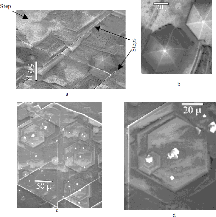
SEM images of the samples’ surfaces are shown in Figs. 3(a)-3(d). The surface of the sample grown on the off-axis seed (Figs. 3a-3b) has a step morphology with several cracks running perpendicular to the steps. There are several highly faceted large hexagonal grains, as shown in Fig. 3(b). The surface of the sample grown on the on-axis seed (Figs 3c-3d) contains many hexagonal grains stacked on top of one another. The surface is flatter than the surface of the AlN grown on the off-axis seed, and the grains are not faceted. Additionally, the top grains are much smaller than those seen on the AlN grown on the off-axis seed.

Fig. 3. SEM images of the samples grown on 3.5° (a-b) off-axis SiC, and (c-d) on-axis SiC. The steps are labeled with arrows.
X-ray results indicate that the AlN grown on on-axis SiC is of better quality than the AlN grown on off-axis AlN. Rocking curve measurements show that the full width half maximum (FWHM) of the (0002) peak for AlN grown on the on axis seed is 5.16 arc-minutes, while the FWHM of the AlN grown on the off-axis seed is 9.6 arc-minutes.
It is interesting to compare the morphology of the AlN grown by physical vapor transport to the AlN films we have grown by MOCVD. Figures 4(a) and 4(b) show (0002) DF images of AlN films grown on on-axis SiC and 3.5° off-axis SiC, respectively. Both films are highly columnar and contain an inversion domain boundary near the surface. These defects hinder the prospect of using these films as buffer layers for high quality nitride film growth.

Fig. 4. (0002) DF images of the AlN films grown on (a) 3.5° off axis SiC and (b) on-axis SiC by MOCVD
Conclusion
The bulk AlN, particularly that grown on the on-axis SiC, shows promising characteristics for the development of this material as a substrate. Further optimization of the growth conditions and a polishing technique to improve the surface quality is needed to yield an AlN surface suitable for high-quality nitride film growth.
Acknowledgements
The authors gratefully acknowledge the support of the MRCP Army Grant No. DAAL 019523530.