


 0) IDB and the (10
  0) SMB and consequently alter the electronic structure of these boundaries.
Introduction
Vacancy and interstitial native defects are known to have a major influence on the electrical and optical properties of GaN [Reference Neugebauer and Van de Walle1]. For example, the N vacancy acts as single donor, the Ga vacancy as an acceptor and the interstitials act as amphoteric defects. The formation energies of native defects in bulk GaN have been calculated using first principles methods and their values are quite well established [Reference Boguslawski, Briggs and Bernholc2, Reference Neugebauer and Van de Walle3]. However, these formation energies will change in the neighbourhood of extended planar defects such as stacking mismatch boundaries and inversion domain boundaries. These boundaries are commonly observed in epitaxially grown GaN but so far the interaction between such interfaces and native point defects in GaN has not been investigated and it remains unclear whether the formation of interstitials and vacancies near the boundaries is encouraged or discouraged.
The calculation of defect-interface interactions requires computational cells containing several hundred atoms so as to avoid unwanted intercellular interactions when periodic boundary conditions are applied. This makes a first principles approach difficult and therefore we have used, in the first instance, a classical methodology which employs interatomic pair potentials that have been fitted to reproduce various bulk properties of GaN. This classical model is used to calculate the binding energy of Ga and N vacancies and interstitials to three commonly observed interfaces: the (10

Figure 1. Observed boundary structures of (a) the (10
Methodology
The computational methodology and pair potential scheme are well established (for a review see Harding [Reference Harding9]) and therefore only a summary is given here. The long range electrostatic energy is evaluated through the Ewald summation [Reference Ewald10]. The interaction between ions at short range is described using Buckingham pair potentials which have the following form:
In a previous study [Reference Chisholm, Lewis and Bristowe11] the potential parameters A, ρ and C were fitted to experimental lattice parameters as well as elastic and dielectric constants. For the N ion, polarisation effects are taken into account using the Shell Model in which the electrons are modelled by a massless ‘shell’ with charge Y which is connected to the core by a spring with spring constant K [Reference Dick and Overhauser12]. The polarisability is then given by α = Y 2/ K.
The use of the supercell approach requires the inclusion of two boundaries per cell. We have carried out convergence tests and found that the following sizes of supercell are more than adequate to eliminate boundary-boundary interactions as well as interactions between native defects: (10
In the pair potential model the atoms are treated as ions in which the Ga atom is attributed a charge of +2 and the N atom a charge −2. The creation of a native defect therefore introduces an overall charge into the supercell. In order to maintain charge neutrality we create an additional native defect. For example, for a N vacancy we also create a Ga vacancy the position of which is kept fixed at the largest possible distance from the N vacancy. Again, the size of the supercells in each case is more than sufficient to eliminate any unwanted defect-defect interactions.
Results
Calculated values for the boundary energies as well as native defect binding energies are shown in table I. The boundary energies compare well with those obtained by Northrup et al [Reference Northrup, Neugebauer and Romano8] who calculated values of 0.025 eV / Å 2 for the (10
Trends for the binding energies can be observed across the boundaries and across the native defects. We note first that for all boundary structures the binding energy is higher for interstitial defects than for vacancies. In bulk GaN, the interstitials have a particularly high formation energy of 5-10 eV (depending on the charge state [Reference Neugebauer and Van de Walle1]) and unlike the case for GaAs, interstitials are not thought to occur in significant concentrations. This result suggests that interstitial defects are more likely to form in the boundary. Indeed, a larger volume of space is available to accommodate interstitials for all three boundaries.
Table 1 Calculated binding energies for Ga and N vacancies and interstitials to three different planar defects. The boundary energy of each planar defect is also given.

In bulk GaN the introduction of a Ga interstitial causes an outward relaxation of the surrounding atoms. The same is generally true for an interstitial introduced into the boundaries. For the case of the (10
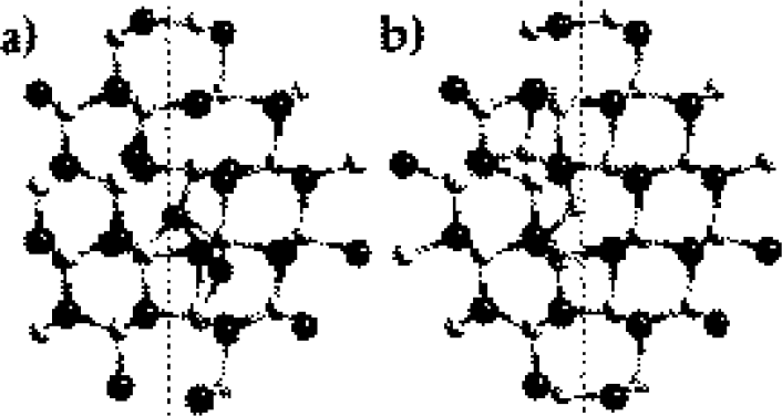
Figure 2. Relaxed structures of (a) the Ga interstitial and (b) the N interstitial in the (101 0) IDB*. Filled and open circles represent gallium and nitrogen atoms respectively. Dashed line indicates the location of the boundary.
A careful comparison of lattice relaxations carried out within a radius of 7 Å for all native defects has shown that displacements are of the same magnitude both in the boundary and in the bulk. Also, it was seen that displacements associated with vacancies are less pronounced than those associated with interstitials. For the Ga vacancy in the (10
The electronic structure of a boundary will be affected by the formation of native defects in its core. In the case of the (10
Conclusions
We have employed a pair potential model to investigate the interaction between native defects and inversion domain boundaries and stacking mismatch boundaries in GaN. The binding energy is found to be positive for all the native defects and boundary structures considered. This indicates that native defects prefer to form in these types of boundary. The binding energy is highest for the Ga interstitial and lowest for the vacancies which can be explained by the larger volume available to accommodate interstitials in the boundary. We conclude that N and Ga interstitials, which do not form in significant concentrations in bulk GaN, should form in the (11
Acknowledgements
Support for this research was provided by the Engineering and Physical Sciences Research Council.


