


1. Introduction
Because of their direct wide band gap, III-V nitrides are of great interest due to their applications in short-wavelength optical devices, or high power and high frequency electronic devices Reference Mohammad, Salvador and Morkoç[1]. The successful development of short wavelength light emitting diodes and the most recent realisation of nitride semiconductor lasers have stimulated great interest in the application of this material for blue and ultraviolet optoelectronic devices. P-type conductivity in GaN is the key for producing the optoelectronics devices. Mg has been widely used Reference Nakamura and Fasol[2] Reference Gotz, Johnson, Bour, McCluskey and Haller[3] Reference Yuan, Salagaj, Gurary, Thompson, Kroll, Stall, Hwang, Schurman, Li, Mayo, Lu, Krishnankutty, Shmagin, Kolbas and Pearton[4] Reference Pearton, Lee and Yuan[5] Reference Amano, Kito, Hiramatsu and Akasaki[6] Reference Nakamura, Mukai, Senoh and Iwasa[7] Reference Pearton, Bendi, Jones, Krishnamoorthy, Wilson, Ren, Karlicek and Stall[8] Reference Smith, Chen, Lin, Jiang, Salvador, Sverdlov, Botchkarev, Morkoc and Goldenberg[9] Reference Gotz, Johnson, Walker, Bour, Amano and Akasaki[10] Reference Yi and Wessels[11] Reference Hacke, Nakayama, Detchprohm, Hiramatsu and Sawaki[12] Reference Johnson, Lin, Jiang, Asif Khan and Sun[13] despite its intrinsic difficulties. It is nowadays well established that during the growth process of Mg doped GaN, atomic H is generated from the decomposition of NH3 and Mg-H complexes are formed in the layer Reference Gotz, Johnson, Bour, McCluskey and Haller[3] Reference Yuan, Salagaj, Gurary, Thompson, Kroll, Stall, Hwang, Schurman, Li, Mayo, Lu, Krishnankutty, Shmagin, Kolbas and Pearton[4] Reference Pearton, Lee and Yuan[5]. This has been for instance shown by the occurrence of LO mode in IR absorption, and recently by the observation of the Mg-H local vibration modes (LVM) Reference Yuan, Salagaj, Gurary, Thompson, Kroll, Stall, Hwang, Schurman, Li, Mayo, Lu, Krishnankutty, Shmagin, Kolbas and Pearton[4] Reference Brandt, Ager, Gotz, Johnson, Harris, Molnar and Moustakas[14]. Measurements of depth profiles showed that Mg and H are incorporated simultaneously Reference Ohba and Hatano[15]. This H passivation limits the electrical activity of Mg, therefore an activation process is required to get full electrical activity of the Mg atoms. Previous difficulties in obtaining high quality p-type films due to the presence of residual impurities and the formation of acceptor-H neutral complex which cause hole compensation have been overcome. Mg-doped p-type GaN is obtained either through low energy electron beam irradiation (LEEBI) Reference Amano, Kito, Hiramatsu and Akasaki[6] Reference Li and Coleman[16] treatment or thermal annealing Reference Nakamura, Mukai, Senoh and Iwasa[7]. The thermal stability of hydrogen-passivated Mg acceptors in GaN depends on the annealing atmosphere. When annealing occurs under nitrogen at T>700°C, hydrogen remains in the material Reference Pearton, Bendi, Jones, Krishnamoorthy, Wilson, Ren, Karlicek and Stall[8]. In this letter, p-doping of GaN and blue-UV LED's were successfully reported using atmospheric pressure metalorganic vapour phase epitaxy.
2. Experimental : growth of Mg-doped GaN
GaN was grown by MOVPE starting from TMG and NH3 as previously described Reference Beaumont, Vaille, Boufaden, el Jani and Gibart[17]. Mg doped GaN layers are grown on (0001) sapphire. Since, like in most heteroepitaxial systems, the buffer layer is of critical importance, we have set up an in situ control of the growth process. Laser reflectometry (LR) was implemented to get an in situ tool for real time diagnosis of the growth process. LR primarily analyses the bulk epitaxial layer, and the information provided by LR is straightforward. During growth of an epitaxial layer with a refractive index different from the substrate, the reflected light intensity follows a periodic function, the period of which is given by

where λ is the wavelength of the laser, n the refractive index of the layer at the growth temperature, V the growth rate and Θ the angle of incidence (normal in our experimental set up). When the light is absorbed (optical absorption by the bulk layer) or scattered by roughening of the surface, the oscillations are damped by a factor α. The experimental set up involves a laser source at 632.8 nm (He-Ne laser) mechanically modulated and a detection system with a synchronous demodulator. Since nitrides are transparent at 632.8 nm, any damping would result from surface roughening.
3. Chemistry
To obtain Mg-doped GaN, two precursors are -a priori- available, the biscyclopentadienylmagnesium (Cp2Mg) and the bismethylcyclopentadienylmagnesium, [(MeCp)2Mg]. (MeCp)2Mg was used in the present study since it has the lowest melting point and the highest equilibrium partial pressure, though Cp2Mg is also commonly used. Both are solid at room temperature, and to avoid any condensation in the piping of the MOVPE reactor, the precursors are kept at 37°C. A careful examination of the growth process reveals that when the (MeCp)2Mg precursor is introduced in the growth chamber, it reacts in the gas phase with NH3 to give solid particles. This was evidenced by a very bright diffuse emission visible along the path of the laser beam used for reflectivity measurements. Most likely, as soon as NH3 and (MeCp)2Mg are mixed together, they react even at room temperature to form new Mg species with different volatilities. These species result from a substitution reactions which proceeds with the elimination of methylcyclopentadiene. The nature of the Mg species resulting from such reactions depends most probably on the temperature and on the stoichiometry, the simplest obvious reaction could be :
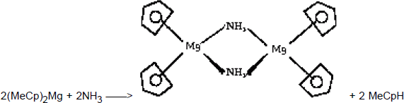
The NH2 ligand is prone to act as an assembling ligand (bridging two or more metals) thus leading to a decrease in the volatility properties Reference Chang, Lec, Her, Lec, Peng and Wang[18]. The reaction between (η5-Cp)2Mg and NH3 could be favoured by a bent structure as observed by electron diffraction (and thus in the vapour phase) for alkaline earth cyclopentadienyle derivative Reference Greenwood and Earnshaw[19] or by intermediates of type (η5−Cp)( η1−Cp)Mg as observed for solid state beryllium compounds (both hypothesis make the metal accessible for co-ordination with ammonia, a likely prerequisite of the substitution reaction Reference Hall, Wolzanski and Van Duyne[20]). To limit this parasitic reaction, the doping line is separated from the Metal Organics manifold, and (MeCp)2Mg is mixed with active gases only in the growth chamber.
As already reported, as grown Mg-doped GaN is highly resistive, therefore not any Hall measurements was achievable. Acceptors can be activated by straightforward annealing in nitrogen atmosphere. It is assumed that Mg-H complexes are destroyed. The thermal annealing is carried out in the MOVPE growth chamber. The Hall data gave values ranging from 2×1017cm−3 and 2×1018cm−3. The annealing process is critical for the activation of Mg acceptors in GaN. Though the SIMS measurements have proven that the Mg incorporation is well controlled, Hall measurement on samples after annealing in similar condition presents scattered results. For a Mg concentration in the lattice of 4×1019cm−3, we obtained measured hole concentrations between 2×10¹⁷ and 2×1018 cm−3. The small mobility values of Mg doped GaN, ranging from 4 to 10 cm2/Vs, induce uncertainty on the hole concentration that can be as high as 100%. But we believe that incomplete annealing is playing the major role. As an example, the RT hole concentration of a sample annealed at 700°C for 30 minutes under N2 at the atmospheric pressure is measured to be 6−8×1017cm−3, but an extra annealing at 750°C for 10 minutes of the same sample has improved this value to 2×1018cm−3 Reference Beaumont, Vaille, Lorenzini, Gibart, Boufaden and el Jani[21].
4. Photoluminescence
PL data on MOVPE GaN samples were already reported Reference Leroux, Beaumont, Grandjean, Massies and Gibart[22]. For Mg-doped samples the evolution of PL with increasing Mg doping is shown on Figure 1. For low Mg doping, the sample is highly compensated, it exhibits either n conductivity or p-type with p~1016cm−3, the spectra is dominated by the shallow donor-acceptor pairs (DAP) bands at 3.27eV. The analysis of the evolution of the DAP peaks with excitation intensity gives acceptor depths of 220 ±5 meV for the acceptor (also observable on PL spectra on undoped GaN sample). However, when increasing the doping level, the PL bands broaden and deepen, as figure 1 shows. For highly p-type doping, the spectra are dominates by a blue band in the 2.7-2.9 eV range, depending of the doping and the excitation intensity. The occurrence of this Mg-related blue band was reported several times and does not depend on the growth method Reference Pearton, Bendi, Jones, Krishnamoorthy, Wilson, Ren, Karlicek and Stall[8] Reference Smith, Chen, Lin, Jiang, Salvador, Sverdlov, Botchkarev, Morkoc and Goldenberg[9].

Figure 1. Luminescence spectra at 9K of undoped and Mg doped MOVPE-grown GaN, with increasing Mg doping levels.
Figure 2 shows a typical low temperature PL ( and reflectivity ) spectrum of a highly Mg-doped GaN sample, and its dependence on the excitation intensity. In addition to the blue band, weak structures near 3.2-3.3 eV can be observed corresponding to DAP bands involving shallow acceptors and donors. The maximum of the 2.8eV bands shifts by 90 meV for two decades of intensity, much higher than would be expected for classical DAP recombinations. Presently, a possible interpretation of the spectra of the Figure 2 is that they involve two overlapping bands, one peaking at 2.7 eV, saturating rapidly with excitation intensity, and a second one peaking at 2.9 eV, observable under high excitation. It should be remember that PL involves minority electrons, and noticing that the shallow DAP bands are also observable under high excitation intensity (Figure 2) suggest that the occurrence of this deep Mg blue band is related to the formation of deep electron states, in agreement with Smith et al Reference Smith, Chen, Lin, Jiang, Salvador, Sverdlov, Botchkarev, Morkoc and Goldenberg[9]. This hypothesis agrees with the general observation that the acceptor thermal depth deduced from Hall data is roughly independent of the doping level. It should also be mentioned that large DAP shifts can be recorded in strongly compensated GaAs. In the case of GaAs these large shifts are interpreted by band structure distortions by inversely charged impurity atoms and concentration fluctuations. On another hand, the reflectivity spectrum displayed in Figure 2 shows that the absorption edge of our sample is in the 3.46-3.47 eV range, thus suggesting that band tailing is not strong. We mention also that the formation of deep donor levels such as Mgi or MgV has been theoretically predicted Reference Neugebauer and de Walle[23]. Clearly, a definitive understanding of the exact nature of PL in highly Mg doped GaN deserves further in depth investigations. As demonstration of the ability of controlling p-doping a LED was fabricated.

Figure 2. Excitation Intensity dependence of the PL spectra at 9K of highly Mg-doped GaN.
5. LED's fabrication
A cross sectional view of a MOVPE grown LED is shown in Figure 3. It consists of a 2μm-thick Si-doped GaN layer (n=2×1018 cm−3) followed by 0.6μm-thick Mg-doped layer (6×1017 cm−3). The hole carrier density was also measured by capacitance and was found to be consistent with the Hall data. Circular mesas with 0.071 cm2 area are formed by dry etching through the p-type GaN:Mg layer until the n-type layer is exposed. The upper contact, 150μm in diameter, is also used as a mask for mesa etching. Au/Ni (1000Å/200Å) and Al/Ni (1000Å/200Å) were used for the n- and p-type contact metals, respectively. Contacts are annealed at 600°C for 5 minutes in N2 ambient. The LED's are mounted on a TO-5 header drilled with a 1 mm hole so that the light can be emitted from the sapphire substrate side of the device.

Figure 3. Cross sectional view of the LED structure.
Figure 4 shows the I-V characteristics of the Mg-doped LED's. We report a forward turn-on voltage of 2.5V. From this curve, the combined effect of the sheet resistance in GaN:Mg and of the specific resistivity of the contact results in a value of about 50W above the turn on voltage. The electroluminescence spectrum of the GaN LED is displayed in Figure 5 together with the standard PL at 300K, and with the PL spectrum of an undoped sample as a reference (lower part of the curve). The upper part of the Figure 5 shows the electroluminescence at low injection current, which is dominated by the blue emission. On another hand, under higher injection, the blue UV emission dominates. Henceforth, the control of n and p-doping of GaN is achieved. This paves the way towards more elaborated structures.

Figure 4. Current-voltage characteristics of blue-UV LED.

Figure 5. Room temperature photo- and electroluminescence of Mg doped layer.
Acknowledgments
The author would like thank M.Vaille, J.C.Guillaume and A.Bouillé for their help with the experiments. This study was supported by an EU contract ESPRIT LTR- LAQUANI 20968.


