1. Introduction
One of the major problems in development of semiconductor devices based on heteroepitaxial films of nitride compounds of type AIIIBV is poor parameter reproducibility and fast degradation of the devices due to the high concentration of crystal structure defects in the films forming the active region. The high defect concentration in these films is due to the large lattice parameters mismatch between adjacent crystal planes of the substrate and of the semiconductor film. For monocrystalline substrates currently used for growing heteroepitaxial (0001) GaN films, the lattice mismatch is 16% for (0001) Al2O3, 9.5% for MgAl2O4, and 3.5% for SiC. A heteroepitaxial buffer sublayer of material with wurtzite crystal structure (GaN, AlN, ZnO) is used to reduce the lattice parameter mismatch when the semiconductor layers are grown on (0001) Al2O3 surfaces Reference Morkoc, Strite, Gao, Lin, Sverdlov and Burns[1]. This large mismatch in the heteroepitaxy of the hexagonal syngony materials with wurtzite structure on the (0001) sapphire surface is due to the 30° in-plane rotation of the contacting (0001) plane of Al2O3 and the (0001) plane of wurtzite relative to each other. The reason for this rotation is that the most dense packing direction in the (0001) plane of Al2O3 is 〈1
00〉 Al
2O
3, and in the wurtzite (0001) plane such direction is 〈1
00〉. According to the criteria of mutual parallelism of the most densely packed directions in the contacting planes in heteroepitaxy, the direction 〈1
10〉 of Al
2O
3 is parallel to the wurtzite 〈1
10〉 direction. The translation period along 〈1
00〉 Al
2O
3 is 2.747Å, while for 〈1
10〉 GaN it is 3.189Å, leading to the large mismatch. Due to the large mismatch, the heteroepitaxial buffer sublayer of the material with wurtzite crystal structure can only grow on (0001) Al
2O
3 by the three-dimensional “island” growth mechanism. As it is known, this growth mechanism only allows for films with the “mosaic” monocrystalline structure, consisting of separate grains with large amount of grain boundaries and high defect concentration. In this article we propose a way to eliminate the 30° in-plane rotation of the (0001) heteroepitaxial A
IIIB
V nitride film with respect to the (0001) or (11
0) working surface of sapphire substrate.
2. Results and Discussion
We noticed that once the 30° in-plane rotation of the (0001) heteroepitaxial nitride film with respect to the substrate is eliminated, the lattice parameter mismatch becomes substantially smaller. Indeed, two translations periods along 〈1
00〉 of Al
2O
3 (2 * 2.747=5.494 Å ) coincides with the 0.5% accuracy with the a single translation along 〈1
00〉 GaN, equal to 5.52Å, and two translations along 〈11
0〉 Al
2O
3, equals 2 * 4.76 = 9.52 Å, this also coincides with three translations along 〈1
10〉 GaN, 3 * 3.189 = 9.56 Å with 0.5% accuracy. To eliminate this 30° in-plane rotation of the film, we propose
Reference Kotelyanskii, Kotelyanskii and Kravchenko[2] to use a buffer sublayer of a material with cubic syngony, which for heteroepitaxy on (0001) or (11
0) Al
2O
3 has the surface orientation {111}, and the direction 〈112〉 in this plane is parallel to the 〈1
00〉 type direction of the Al
2O
3, lying in the working surface of the substrate. When a wurtzite type material is further grown on the {111} surface of the cubic syngony material, the following epitaxial relationships hold:
-
{111} planes of the cubic lattice and (0001) planes of wurtzite are parallel;
-
〈112〉 directions of the cubic lattice and 〈1
00〉 directions of wurtzite are parallel.
Thus, if materials with cubic syngony are used for the buffer sublayer, the following orientation relationships can be obtained:
in both cases: 〈1
00〉 Al
2O
3 ∥ 〈112〉cubic ∥ 〈1
00〉wurtzite.
Thus, if the buffer sublayer is prepared as we propose from material with crystalline structure of cubic syngony, with the lattice unit cell parametera such that the translation length along the 〈112〉 direction of this lattice is very close to a multiple of the translation lengths along the 〈1
00〉 directions in the semiconductor film and in the substrate, an almost perfect lattice parameter match can be achieved, for instance, between (0001) Al
2O
3 and {111} of the buffer layer on one side, and {111} of the buffer sublayer and (0001) of the film with wurtzite structure, on the other side.
The cubic lattice unit cell parameter of the buffer sublayer material a can then be determined from the relationship a* 20.530.5 = n * 2.747Å , where 2.747Å is the translation period along 〈1
00〉 Al
2O
3, and
n is an integer; this gives
a=1.125
nÅ. The unit cell lattice parameters of the Ga and Al nitrides, as well as solid solutions of Ga, In, and Al, used in semiconductor devices, are within the range from 3.11 to 3.25Å . Materials with a unit cell parameter
a less than 2.5Å , or greater, than 13Å are practically absent. A reasonable choice would be to use as buffer sublayers materials with cubic syngony with the value of
a ~1.125
n Å, where
n equals 3, 4, 6 or 8. Values of 5, 7, or 9 are not acceptable for
n, as in these cases translations along 〈112〉 and 〈110〉 of the (111) buffer layer plane, are not multiples of the translations along 〈1
00〉 and 〈11
0〉 of the semiconductor film. These values do not allow achievement of the desired result. Notice that in the case of heteroepitaxial deposition of semiconductor nitride film with the zinc blende polytype structure, the material of the heteroepitaxial buffer sublayer should also be chosen according to the conditions described above. Heteroepitaxial buffer sublayers can be implemented using material with cubic syngony with the crystal lattices of various types, like for instance α-Fe, NaCl, and spinel. Sublayer materials can be dielectrics such as BaCeO
3, MgO, and BP, conducting materials such as nitrides and carbides of niobium, hafnium, scandium, titanium and their solid solutions, or metals like niobium and tantalum. Buffer sublayers made of conducting material, can in addition serve as one of the electrodes of a semiconductor device. Heteroepitaxial layer structures may contain several buffer sublayers.
Our experiments show that using a {111} niobium heteroepitaxial buffer sublayer allows the elimination of the 30° in-plane rotation of (0001) Al2O3 with respect to the (0001) AlN film. The lattice parameter misfits along the mutually parallel 〈1
00〉 Al
2O
3 ∥ 〈112〉 Nb and 〈11
0〉 Al
2O
3 ∥ 〈110〉 Nb directions are less than 2%. A very thin film of niobium nitride formed subsequently on the surface of the niobium buffer sublayer and the (0001) aluminum nitride film grown on it has practically coinciding (within 0,1% accuracy) atomic plane lattices.
The 30° in-plane rotation between 〈1
00〉 Al
2O
3and 〈1
00〉 AlN for (11
0) sapphire substrates can also be removed by using {111} niobium nitride barrier layer. The lattice parameter misfit is less than 2% along the mutually parallel 〈1
00〉 Al
2O
3 and 〈112〉 NbN directions, and (0001) AlN films grown on it have practically coinciding atomic plane lattices.
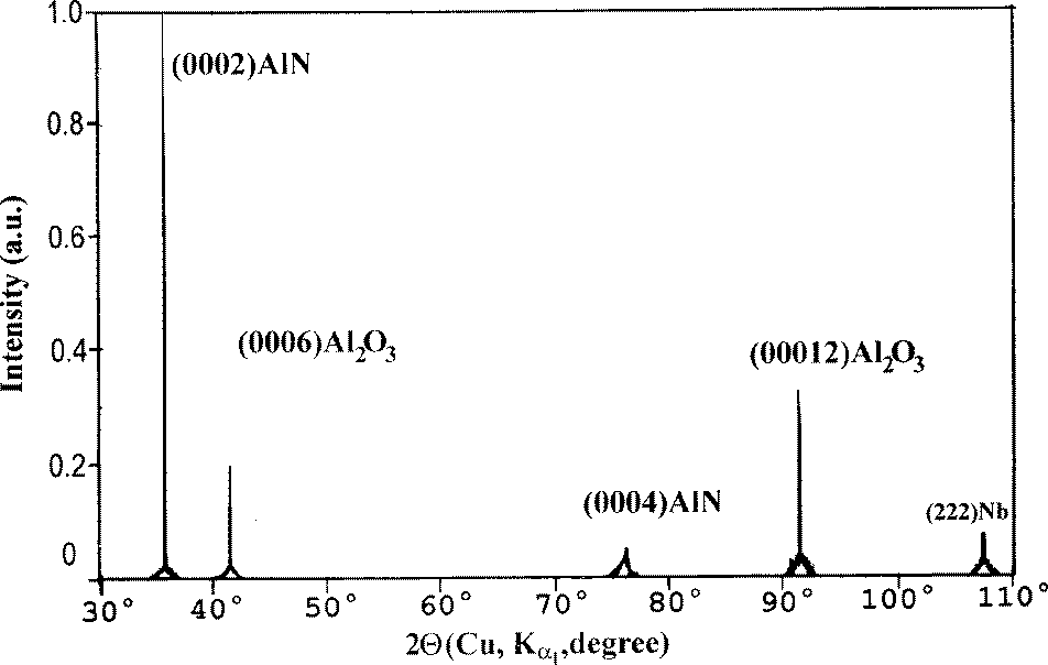
Heteroeptaxial Nb, NbN and AlN thin films on (0001) and (11
0) sapphire substrates were deposited by the RF- magnetron sputtering method. The orientations of the films relative to the substrate was investigated by X-ray diffraction analysis; standard Θ − 2Θ diffractometry and φ − scans for pole figure drawing. We used a double-crystal diffractometer DRON-3 (Cu, K
α1 X-ray tube). The XRD pattern of AlN grown on a Nb sublayer and on a (0001) Al
20
3 substrate is presented in
Figure 1.
Figure 2 shows the representative X-ray pole figures from AlN, Nb films and (0001) Al
20
3 substrate.
Figure 2 (a,b,c) are pole figures taken for peaks from AlN -{10
1}, Nb -{200} and Al
20
3- {01
2}, respectively. The results indicate that the in-plane orientations between (0001) AlN and (0001) Al
20
3 changed when a Nb intermediate epitaxial layer is formed on the substrate. The appearance of six spots in
Figure 2(b) for Nb{200} planes can be explained by the occurrence of the double positioning of the Nb film.
Figure 1. XRD (Θ-2Θ) scan of AlN film, growth on Nb sublayer and (0001) Al2O3 substrate.
Figure 2. Representative X-ray pole figures from: a) (0001) AlN film (pluses) - peaks {10
1}; b) (111) Nb film (filled circles) peaks {200} c) (0001) Al
2O
3 substrate (triangles) - peaks {0
12}
The orientation relationships were found to be the following:
and
Notice, that the orientation relationships we obtained between the heteroepitaxial {111}Nb layer on (0001)Al203and {111} NbN on (11
0) Al
20
3 are in agreement with earlier published experimental results presented in
Reference Masek and Matolin[3] and
Reference Noskov, Titenko, Korzhinsky and Komashko[4] correspondingly.


 0) working surface of the sapphire substrate. In these cases, the lattice parameter mismatch between the sapphire substrate surface and the semiconductor film is much smaller, and the cleavage planes of the sapphire and the semiconductor films with wurtzite structure forming the active region of a heterolaser are parallel. It is shown experimentally that using, for instance, Nb on (0001) Al