


1. Introduction
Recently the group III-nitrides (In, Ga)N have attracted much attention because of the high potential for the fabrication of light emitting devices operating in the red to ultraviolet wavelength range. Despite the recent success in realizing devices, only few reports have been made on growth of InGaN. In this paper growth of high quality InGaN films on (0001) sapphire substrates by atmospheric pressure organometallic vapor phase epitaxy in a close spaced vertical rotating disk reactor is investigated. The effect of several growth parameters on the indium incorporation and the optical quality of InGaN films and InGaN/GaN quantum wells is investigated. The layers are characterized by optical microscopy, DC X-ray and 300 K photoluminescence measurements.
2. Experiment
InGaN films and quantum wells were grown by metalorganic chemical vapour deposition on two inch sapphire (0001) substrates with nitrogen carrier gas. Ammonia (NH3), trimethyl-gallium (TMG) and trimethyl-indium (TMI) were used as source materials. The growth was conducted in a close spaced vertical rotating disk reactor, manufactured by Thomas Swan & Co Reference der Stricht, Moerman, Demeester, Crawley and Thrush[1] Reference Van der Stricht, Moerman, Demeester, Crawley and Thrush[2]. Deposition was performed under atmospheric pressure. The InGaN films were deposited on 2 micron thick GaN layers, because the lattice constant of InGaN is closer to GaN then sapphire. The growth was performed with a high indium source flow rate and nitrogen carrier. This is necessary because the indium incorporation is very low at growth temperatures in the range of 700 to 850 °C Reference Nakamura, Mukai and Senoh[3]. Typical flow rates for carrier, NH3 TMG and TMI are 4 l/min, 2.5 l/min, 5.6 μmol/min and 22.7 μmol/min. The V/III ratio was varied between 5200 and 5900. The thickness of the InGaN bulk layers varied between 0.4 and 0.2 micron. The InGaN quantum wells were imbedded in GaN layers grown at low temperatures, where the top layer has to prevent the decomposition of the quantum well while ramping up to 1050 °C (GaN growth temperature). The InGaN films were characterised by X-ray measurements to examine the crystal quality. For this a Bede double crystal (DC) diffractometer set-up was used. Optical characterisation was performed by photoluminescence (PL) measurements, where the 325 nm line of a HeCd-laser was used to excite the samples. The characterized InGaN/GaN structures are shown in Figure 1.
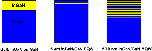
Figure 1. Characterized InGaN structures.
3. Results
3.1 Indium incorporation
The main problem with InGaN growth is that low growth temperatures are required to achieve a high indium incorporation, because of the high indium volatility at temperatures above 1000 °C Reference Matsuoka, Yoshimoto, Sasaki and Katsui[4]. Lowering the growth temperature however usually results in an inferior material quality, because at temperatures below 1000 °C the decomposition rate of NH3 is very low. Recently Flow Modulation Epitaxy has been introduced to grow InGaN films, taking advantage of surface catalytic effects, to achieve a higher quality Reference Keller, Mishra and DenBaars[5] Reference Lu, Thothathiri, Wu and Bath[6]. However it would be preferable not having to resort to such complex growth processes. Consequently the incorporation efficiency of indium is an important measure for the MOVPE reactor suitability for producing nitride based light emitting devices. To estimate the incorporation efficiency the indium composition of thick (200 to 400 nm) InGaN films was determined for several growth temperatures. (Figure 2) The indium incorporation decreases drastically for increasing growth temperature. For a higher V/III ratio the indium incorporation seems to increase slightly. The indium incorporation is also influenced by the growth rate: for higher rotation speeds (leading to higher growth rate) the indium content of the grown InGaN films was slightly lower. The composition of a InGaN film can thus be controlled by varying the following three parameters: growth temperature, V/III ratio and rotation speed. All in all the closed spaced vertical rotating disk reactor configuration seems to result in a very high growth efficiency for InGaN material, compared to other configurations. InGaN layers with an indium composition up to 56 % have been deposited which still exhibit very good optical properties, as discussed further on.
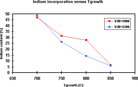
Figure 2. Indium incorporation versus growth temperature.
3.2 Morphology
When attempting to grow high quality InGaN films with a high indium composition the formation of indium droplets on the surface is a frequent problem. Typically the amount of indium droplets increases exponentially with the reduction of growth temperature Reference Sun, Yang, Chen, Lim, Anwar, Khan, Temkin, Weismann and Brenner[7]. The surface of the InGaN films discussed in this paper were studied with an optical microscope. At growth temperatures below 750 °C the complete surface was covered with metal droplets. The film showed a gray color to the naked eye. Between growth temperatures of 750 to 800 °C the surface had a yellow appearance. Above 800 °C the surface was almost featureless and transparent. By increasing the V/III ratio from 5200 to 5900 the indium droplet formation could be reduced slightly.
3.3 Double Crystal X-ray Diffraction
To determine the crystalline quality of the InGaN films some DC X-ray measurements were carried out. For the InGaN bulk layers two clearly resolved peaks could be distinguished in the rocking curves: a narrow peak for the underlying GaN and a broader peak originating form the InGaN top layer. The FWHM of the InGaN rocking curve varied between 8 and 15 arcmin. For the MQW structures an average InGaN composition shoulder was clearly visible on the GaN peak, but no satellite peaks were detected so far (Figure 3).
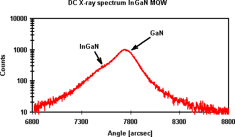
Figure 3. DC X-ray spectrum of InGaN/GaN MQW structure.
3.4 Photoluminescence (300 K)
The indium composition in the previously discussed InGaN films was calculated from room temperature photoluminescence measurements (assuming a band bowing parameter of 1 eV). Figure 4 shows some typical PL spectra for InGaN films with different indium content (from 9 to 56 %). All the spectra show an intense band edge emission and a weak broad emission band. The broad band emission most probably originates from nitrogen vacancies. The creation of these deep levels is a consequence of the decreased NH3 decomposition at the InGaN growth temperatures. This theory was confirmed by the following observation. When increasing the NH3 flow the ratio band edge (BE) to deep level (DL) emission increased significantly. For a NH3 flow rate of 2.5 slm the ratio BE/DL was 2, for a flow rate of 3 slm the ratio BE/DL increased over 4. The BE/DL ratio was higher for InGaN films with a low indium content. Remarkably is that even for the InGaN film with 56 % indium content the PL band edge peak is still quite intense and narrow. However, the intensities have been normalized for comparison. Normally the BE emission intensity decreases with increasing indium composition. The FWHM of the BE peak typically increases linearly with indium composition between 100 and 200 meV for InGaN layers with a indium content of 9 and 56 % respectively (Figure 5). When the InGaN layers are doped with Si the DL luminescence intensity decreases. In Figure 6 the room temperature PL spectra of a Si doped and undoped InGaN with the same In-content are compared. For the Si-doped InGaN layer hardly any DL luminescence is detected.

Figure 4. PL spectra of InGaN films with different indium composition
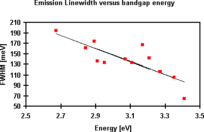
Figure 5. Emission linewidth of InGaN versus band gap energy.
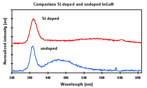
Figure 6. PL spectra of Si-doped and undoped InGaN bulk layers.
3.5 InGaN/GaN QW structures
A InGaN/GaN SQW and bulk InGaN luminescence spectrum are shown in Figure 7. At 365 nm a weak GaN peak is detected. The SQW emission is quite broad and is overlapping with a very intense deep level emission band. The calculated indium composition for the well is approximately 35 %. A higher indium composition is usually found for the QW's than the bulk layers grown under the same conditions, as reported previously by other groups. Reference Nakamura, Senoh, Iwasa, Nagahama, Yamada and Mukai[8]. However more experiments are needed to quantify this effect more accurately. The defect related emission is much stronger for the InGaN/GaN QW than the InGaN bulk layers. However it is highly possible that the DL emission is generated in the GaN barriers instead of the QW, because GaN layers grown at low temperatures are commonly of inferior quality due to nitrogen vacancies Reference Keller, Keller, Kapolnek, Abare, Masui, Coldren, Mishra and Den Baars[9]. The InGaN/MQW structures (Figure 8) show a more intense and more narrow emission peak, but this partially related to the lower indium composition. Doping the InGaN/GaN QW structures with Si should result in a higher luminescence intensity and decreased DL emission. Finally the GaN barrier quality must be improved to achieve device quality InGaN/GaN QW's.
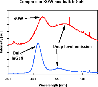
Figure 7. PL spectra of InGaN/GaN SQW bulk InGaN structures.

Figure 8. PL spectrum of InGaN/GaN MQW structure.
4. Conclusion
InGaN films were grown in a close spaced vertical rotating disk reactor. The layers showed narrow DC X-ray rocking curves, intense PL band edge emission and only weak deep level related emission. InGaN with an indium composition up to 56 % have been grown, retaining good optical quality. Preliminary results on InGaN/GaN QW growth are very promising.
Acknowledgments
Wim Van der Stricht thanks the IWT for financial support and Samuel Mertens for carrying out PL measurements in the framework of his undergraduate thesis


