N polarity). These planar defects exhibit the characteristics of stacking faults with a shift vector of a 1/3 [1
Introduction
Obtaining efficient p-type doping has been a continual challenge in GaN technology. GaN can easily be grown with n-conductivity but obtaining p-doping is more difficult. The most commonly used p-dopant is Mg. Despite the success in using Mg as p-dopant to fabricate light emitting diodes (LEDs) and lasers [Reference Nakamura, Senoh and Mukai1], many aspects of Mg-doping in GaN are still not understood. We report here evidence that, under certain growth conditions, Mg segregates and causes formation of several different types of defects depending on the details of the growth condition and on the growth polarity.
Experimental
Three different types of samples were studied: bulk samples, MOCVD samples with Mg delta doping and MOCVD samples where Mg was added continuously. The bulk Mg doped GaN crystals were grown by the High Nitrogen Pressure Method from a solution of liquid gallium containing 0.1−0.5 at.% Mg [Reference Porowski, Bockowski, Lucznik, Grzegory, Wroblewski, Teisseyre, Leszczynski, Litwin-Staszewska, Suski, Trautman, Pakula and Baranowski2]. P-type conductivity was not achieved in these crystals, all were highly resistive.
The Mg delta-doped structure was grown at 1030°C by MOCVD at 200 Torr in a hydrogen (H2) ambient using trimethylgallium (TMGa) and ammonia (NH3). Cp2Mg was used as the Mg precursor. The superstructure of a 130-period GaN/Mg delta doped layer consisted of 104 Å-thick layers of GaN, each followed by a 15 second exposure of Cp2Mg. During the Cp2Mg exposure, the TMGa was vented, but the NH3 and H2 remained flowing into the chamber. At the end of the growth samples were in`-`situ annealed at 850°`C for 10 min in order to dissociate Mg-H complexes and activate the Mg atoms.
The p-i-n structures were also grown by MOCVD at the same temperature (1030°C) but with continuous Cp2Mg exposure and similar growth rate (5.5 Å/s) compared to (5.3Å/s) used for the delta doping. The same annealing at 850°C for 10 min was also performed. All crystals have been studied using transmission electron microscopy (TEM). Dopant concentration and impurity levels were determined using Secondary Ion Mass Spectrometry (SIMS) and Energy Dispersive x-ray spectroscopy (EDX). Crosssection samples were prepared along the [1![]() 100] direction for Convergent Beam Electron Diffraction (CBED) in order to determine crystal polarity and along the [11
100] direction for Convergent Beam Electron Diffraction (CBED) in order to determine crystal polarity and along the [11 ![]() 0] direction for high resolution cross-section studies (HREM).
0] direction for high resolution cross-section studies (HREM).
Results
Fig.1a shows a high resolution image of cross-sectional TEM micrograph from the the bulk sample B together with a ball model (Fig. 1b) indicating that this part of crystal was grown with [000![]() ] N polarity. This figure shows the presence of planar defects separated from each other by equal distances about 10.4 nanometers (20 c-where c is the lattice parameter). Selective area diffraction patterns (SAD) show that the formation of these regularly spaced planar defects leads to additional diffraction spots dividing the (0001) reciprocal distance into 20 equal parts (Figs.1c, d). Our earlier studies of these defects show that these monolayers have a 1/3 [1
] N polarity. This figure shows the presence of planar defects separated from each other by equal distances about 10.4 nanometers (20 c-where c is the lattice parameter). Selective area diffraction patterns (SAD) show that the formation of these regularly spaced planar defects leads to additional diffraction spots dividing the (0001) reciprocal distance into 20 equal parts (Figs.1c, d). Our earlier studies of these defects show that these monolayers have a 1/3 [1![]() 00]+c/2 displacement vector [Reference Liliental-Weber, Benamara, Washburn, Grzegory and Porowski3-Reference Liliental-Weber, Benamara, Swider, Washburn, Grzegory, Porowski, Lambert, Dupuis and Eiting5] characteristic of a stacking fault. However, a splitting of the (0001) and (0003) reflections (Fig.1e) indicates that these defects contain inversion domain boundaries (IDBs). This was also confirmed by a multi-beam dark field image obtained from the [11
00]+c/2 displacement vector [Reference Liliental-Weber, Benamara, Washburn, Grzegory and Porowski3-Reference Liliental-Weber, Benamara, Swider, Washburn, Grzegory, Porowski, Lambert, Dupuis and Eiting5] characteristic of a stacking fault. However, a splitting of the (0001) and (0003) reflections (Fig.1e) indicates that these defects contain inversion domain boundaries (IDBs). This was also confirmed by a multi-beam dark field image obtained from the [11 ![]() 0] zone axis. By placing either (0001) or (000
0] zone axis. By placing either (0001) or (000![]() ) diffracted beams on the zone axis with a small objective aperture reverse contrast on the defects was obtained. This confirms that these defects contain inversion domain boundaries (IDBs).
) diffracted beams on the zone axis with a small objective aperture reverse contrast on the defects was obtained. This confirms that these defects contain inversion domain boundaries (IDBs).

Fig. 1. (a) High magnification of sub-surface area, grown in the N polar directionindicated by ball model shown in (b), showing periodic arrangement of planar defects; (c) fraction of the diffraction pattern between (1![]() 00) and (1
00) and (1![]() 01) diffraction spots showing formation of satellite spots due to formation of ordered structure; (d) intensity distribution through this pattern showing division of (0001) reciprocal distance into 20 equal spacings; (e) A splitting of (0001) reflection.
01) diffraction spots showing formation of satellite spots due to formation of ordered structure; (d) intensity distribution through this pattern showing division of (0001) reciprocal distance into 20 equal spacings; (e) A splitting of (0001) reflection.
EDX analysis [Reference Liliental-Weber, Benamara, Washburn, Grzegory and Porowski4] with an electron beam size of the order of 1 nm which was placed either on the defect or in the area between the defects confirmed that these planar defects are Mg rich. The ordering close to the N polarity surface was not observed in all studied crystals, such as Ba and P (Table I). In some of them only partial ordering took place and thick layers of regular hexagonal material were present between ordered areas (not shown for lack of space). Some specimens had no ordering at all. This suggests that the ordered structures form only for certain critical growth conditions.
Table I: Dopant and impurity concentration based on SIMS studies
| Sample | Mg ( cm−3 ) | O (cm−3) | C (cm−3) | Si (cm−3) |
|---|---|---|---|---|
| B | 6e19 | 2.5e19 | 1.5e17 | 4e16 |
| M | 5e19 | 3e19 | 5e17 | 1e16 −1e17 |
| Ba | 4−6e19 | 7e19 | 1.5e18 | 1−2e19 |
| P | 3e19 | <3e18 | 2−10e17 | 1−10 e16 |
| MOCVD | 1.5−3e19 | 5e16 | 5e16 | |
| MOCVD | 3e19 | 5e16 | 5e16 |
This opposite side of the bulk crystals (Ga-polarity) had a completely different defect structure as shown in (Fig. 2a). They appear in [11 ![]() 0] cross-section TEM micrographs as triangular features with a base on (0001) c-planes and six {11
0] cross-section TEM micrographs as triangular features with a base on (0001) c-planes and six {11 ![]() 2} side facets. All these triangles were oriented in a direction with the base closest and parallel to the sample surface with Ga-polarity, e.g. from the triangle tip to the base a long bond direction along the c-axis is from Ga to N. No additional diffraction spots (or satellite spots) were observed on this side of the crystal (Fig. 2b).
2} side facets. All these triangles were oriented in a direction with the base closest and parallel to the sample surface with Ga-polarity, e.g. from the triangle tip to the base a long bond direction along the c-axis is from Ga to N. No additional diffraction spots (or satellite spots) were observed on this side of the crystal (Fig. 2b).

Fig. 2. (a) Tetrahedral-shaped defects formed in bulk GaN crystals grown with Ga polarity, (b) Fraction of the diffraction pattern between (1![]() 00) and (1
00) and (1![]() 01) diffraction spots obtained from this area of the crystal. Note lack of satellite spots; (c) Defects observed in plan-view configuration indicating that they are empty inside; (d) Another type of hollow defect (in cross-section) formed for growth with Ga polarity.
01) diffraction spots obtained from this area of the crystal. Note lack of satellite spots; (c) Defects observed in plan-view configuration indicating that they are empty inside; (d) Another type of hollow defect (in cross-section) formed for growth with Ga polarity.
These triangular defects were observed in many of the bulk samples. The dimensions of the largest defects are in the range 100 nm (measured length of their bases) and the smallest are about 3−5 nm. The density of these defects is about 2.5×109cm−2. Studies in the plan-view configuration confirm that these defects are pyramids and that they are empty inside (Fig. 2c). CBED studies of these defects indicate that some reconstruction exist on the internal surfaces of these pinholes most probably caused by Mg segregation [Reference Liliental-Weber, Benamara, Swider, Washburn, Grzegory, Porowski, Lambert, Dupuis and Eiting5]. There were also crystals like M and Ba (see Table I) where these defects were not observed at all. Especially for crystal Ba in which there were no structural defects at all despite the fact that Mg concentration was comparable to those where ordering was present (B and M) and where highest concentration of oxygen was observed. A second type of hollow defect (empty inside) was also observed in cross-section samples, a rectangular defect delineated by a cubic layer on top and bottom basal plane of internal surfaces (Fig. 2d). The different types of defects observed on the crystal sides grown with N and Ga-polarity is likely to be associated with different surface reconstructions and different positions within the unit cell where the Mg atoms are incorporated.
These different types of defects (planar and three-dimensional) formed for growth with different polarities were observed initially in bulk crystals doped with Mg [Reference Liliental-Weber, Benamara, Washburn, Grzegory and Porowski3-Reference Liliental-Weber, Benamara, Swider, Washburn, Grzegory, Porowski, Lambert, Dupuis and Eiting5], where many crystals are grown during a single growth run, and the precise growth condition for each particular crystal is rather indeterminate. Therefore, experiments were also carried on heteroepitaxial samples grown by MOCVD, where the growth conditions can be controlled for each crystal.
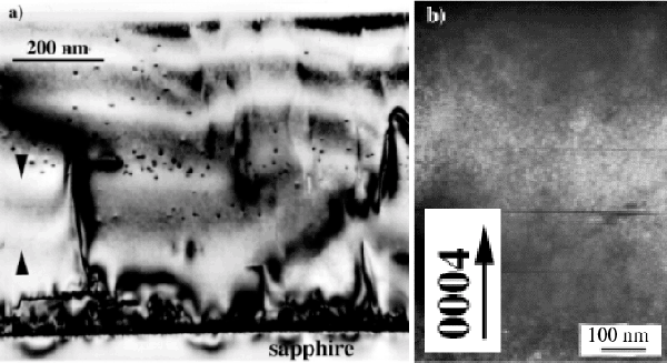
TEM studies on cross-section Mg-delta doped samples also show both types of defects formed for the two opposite polarities in bulk GaN:Mg, e.g. planar defects (polytypoids) which were characteristic for growth with N polarity and pyramidal and rectangular pinholes observed in the bulk GaN:Mg grown with Ga polarity (Fig. 3). This observation clearly suggests that crystal growth polarity is changing due to Mg doping in agreement with earlier studies [Reference Ramachandran, Feenstra, Sarney, Salamanca-Riba, Northrup, Romano and Greve6].

Fig. 3. (a) Cross-section micrograph from the MOCVD grown GaN sample with Mg-delta doping. Note high density of triangular and also rectangular defects typical for growth with Ga polarity. The arrows show the area where planar defects are formed typical for N polarity. Their higher magnification of the area with planar defects is shown in (b).
Fig. 3a shows that growth of about 150 nm of GaN:Mg above the buffer layer did not have any visible change in defect arrangement compared to undoped samples [Reference Liliental-Weber, Benamara, Washburn, Grzegory and Porowski3]. However, in the following layer, about 200 nm thick, planar defects, like those in GaN:Mg bulk crystals grown with N-polarity was observed (Fig. 3b). In the layer following these planar defects a high density (∼ 1010 cm−2) of triangular and rectangular defects like those observed in bulk crystals grown with Ga polarity was observed. SIMS analysis shows (Fig. 4a) much higher Mg concentration (4×1019 cm−3) present in the areas where ordering took place. At the layer thickness at which the hollow defects (rectangular and triangular) were formed Mg concentration dropped to 2×10¹⁹ atoms/cm3 and stayed almost constant with a slow increase to reach a concentration of 4×1019 cm−3 at the sample surface. Impurity levels in this sample were very low showing carbon and oxygen concentrations on the level of 4−5×1016 cm−3 (three orders of magnitude lower than in the bulk samples), therefore, defects which were formed in these crystals must be caused by the Mg presence rather than by oxygen impurity level.

Fig. 4. (a) SIMS measurements obtained from a MOCVD sample with Mg delta doping. A higher Mg concentration was measured in the area where planar defects were formed, similar to those observed in the bulk GaN:Mg, (b) Similar analysis for the sample with continuous Mg doping where formation of structural defects was not observed despite the comparable Mg concentration.
However, in a sample where Mg was supplied continuously, despite similar Mg concentration (Fig. 4b), similar impurity levels and practically the same growth rate, formation of the previously described planar and/or three-dimensional defects was not observed. Therefore, it is not surprising that not all bulk samples showed ordering, since some deviations in composition, temperature or growth rate are possible from crystal to crystal growing in different parts of the container.
Summary
Ordering observed in GaN:Mg for growth with N-polarity appears to be similar to the polytypoids formed in AlN rich in oxygen, or in Mg-Al-N-O-Si compounds [Reference Jack7-Reference Yan, Terauchi and Tanaka8]. Different types of polytypoids were observed depending on the M/X ratio (M-metal and X-nonmetal). In all these samples oxygen concentration was at a level close to 1 at. % or higher [Reference Jack7-Reference Yan, Terauchi and Tanaka8]. In our bulk samples oxygen concentration was high, but only in the range of 5×1019 cm−3. However, in the samples with Mg delta doping oxygen concentration was only at the level of 5×1016 cm−3, therefore, the polytypoids which are formed in our GaN:Mg samples are probably not oxygen related. It is anticipated that they must be caused most by the Mg presence, which was confirmed by EDX studies [Reference Liliental-Weber, Benamara, Washburn, Grzegory and Porowski4]. Our experimental observations indicate that planar defects formed for growth with N polarity show a shift of 1/3 [1 ![]() 00] +c/2 and contain an inversion. Different Mg behavior for N-and Ga-polarity can be expected based on the theoretical work of Bungaro et al [Reference Bungaro and Bernholc9], but ordering was a rather unexpected finding. Segregation of Mg was expected for N-polarity, but the present studies show that for specific growth conditions Mg segregation can also occur for Ga polarity. The presence of Mg also leads to formation of hollow defects in the form of pyramids and rectangular defects with surface reconstruction due to Mg segregation. This indicates that Mg segregated on particular planes tends to prevent further growth. These three dimensional defects were observed in the majority of bulk GaN samples but also in GaN:Mg delta doped samples grown by MOCVD.
00] +c/2 and contain an inversion. Different Mg behavior for N-and Ga-polarity can be expected based on the theoretical work of Bungaro et al [Reference Bungaro and Bernholc9], but ordering was a rather unexpected finding. Segregation of Mg was expected for N-polarity, but the present studies show that for specific growth conditions Mg segregation can also occur for Ga polarity. The presence of Mg also leads to formation of hollow defects in the form of pyramids and rectangular defects with surface reconstruction due to Mg segregation. This indicates that Mg segregated on particular planes tends to prevent further growth. These three dimensional defects were observed in the majority of bulk GaN samples but also in GaN:Mg delta doped samples grown by MOCVD.
An extremely interesting observation in this study, that deserves further investigation, is that in the MOCVD layers grown under similar conditions and with similar Mg concentration, but where Mg is introduced continuously rather than using the delta doping process, none of the defects were formed. Since growth of MOCVD layers can be better controlled than bulk growth this can lead to further understanding of the behavior of Mg in GaN structures. Optimum growth conditions may be identified which result in active dopant as needed for p-type conductivity but which avoid formation of defects. Formation of these structural defects for Mg doped samples helps to explaining why consistent p-doping has been rather difficult.
Acknowledgements
This work was supported by U.S. Department of Energy, under the Contract No. DEAC03-76SF00098. The use of the facility at the NCEM at LBNL is greatly appreciated. Work at UT-Austin was supported by the ONR under N00014-95-1-1302 (monitored by Dr. J. C. Zolper) and the NSF under Grant CHE-89-20120.