Introduction
Group III-Nitride-Arsenides are promising materials for 1.3μm and 1.55μm telecommunications optoelectronic devices grown on GaAs substratesReference Coldren, Larson, Spruytte and Harris 1 , Reference Nakahara, Kondow, Kitatani, Larson and Uomi 2 , Reference Coldren, Spruytte, Marshall, Harris and Larson 3 . The role of nitrogen is two fold: the nitrogen causes the bulk bandgap to decrease dramatically and the smaller lattice constant of GaN results in less strain in InGaNAs compared to InGaAs. However, the growth of such nitride-arsenides is complicated by the difficulty of generating a reactive nitrogen source and the divergent properties of nitride and arsenide materials. The luminescence properties of InGaNAs deteriorate rapidly with increasing nitrogen concentrationReference Coldren, Spruytte, Marshall, Harris and Larson 4 . It is common to increase the luminescence efficiency of these InGaNAs quantum wells by a short high temperature annealReference Coldren, Spruytte, Marshall, Harris and Larson 3 .
In the present study, growth of nitride-arsenides was performed by elemental source MBE using a rf nitrogen plasma. We have investigated the incorporation of nitrogen using X-Ray photoelectron spectroscopy (XPS), secondary ion mass spectroscopy (SIMS), high resolution X-ray diffraction (HRXRD), and electron microprobe. The effect of thermal annealing on crystal quality and nitrogen incorporation was studied using XPS and HRXRD.
Details of MBE Nitride-Arsenide Growth
The growth of Nitride-Arsenides was performed in a Varian Gen II system by elemental source MBE. Group III fluxes are provided by thermal effusion cells, dimeric arsenic is provided by a thermal cracker, and reactive nitrogen is provided by an rf plasma cell. The plasma cell is operated at 250−350 W with a nitrogen gas flow of 0.1−0.5 sccm. Typical growth rates are 0.4−4 Å/s. These conditions allow to add up to 5 atomic percent nitrogen to III-V materials.
To minimize ion damage to the surface of the growing film, an rf plasma is used to generate atomic nitrogenReference Kirchner, Heinke, Birkle, Einfeldt, Hommel, Selke and Ryder 5 . The exit aperture of this source was custom designed so that the plasma can operate with low nitrogen flow rates without compromising the uniformity of the generated atomic nitrogen. The plasma conditions that maximize the amount of atomic nitrogen versus molecular nitrogen were determined using the emission spectrum of the plasma (see Figure 1). The intensity of the first set of bands at approximately 550, 580, and 650 nm is a measure of the amount of molecular nitrogen; the intensity in the bands at 740, 820 and 870 nm is proportional to the amount of atomic nitrogen present in the plasmaReference Park 6 . Both the ratio of atomic nitrogen versus molecular nitrogen and the total amount of atomic nitrogen created, increase with increasing plasma power. For our plasma source design, the plasma power is more effective than the nitrogen flow rate to control the generation of atomic nitrogen. We optimized the start-up procedure of the plasma to maximize the generation of atomic nitrogen.

Figure 1. Emission spectrum of the rf nitrogen plasma for an nitrogen supply of 0.25 sccm and power of 300 W.
We have verified with SIMS that the impurity concentration (H, O, C and B) in our films is below 2.1017/cm3.
Study of Nitrogen Incorporation
For the plasma operating with 300 W power and 0.25 sccm nitrogen flow, the nitrogen concentration in the film is dependent on the gallium arsenide (GaAs) growth rate as shown in Figure 2. The nitrogen concentration is inversely proportional to the GaAs growth rate because the atomic nitrogen is so reactive that all the supplied atomic nitrogen is consumed to form GaNAs. N2 formation is limited because the generated amount of atomic nitrogen is small compared to the As2 and Gallium overpressures in the MBE systemReference Qui, Nikishin, Temkin, Elyukhin and Kurdriavtsev 7 . As the films are grown under an As2 pressure of twenty times the gallium pressure, the GaAs growth rate is only dependent on the Gallium flux. Therefore, the nitrogen concentration of the InGaNAs films can be controlled solely by the group III flux. This indicates that the InGaNAs system might have some advantages in terms of yield and reproducibility compared to the arsenide-phosphide system where the group V flux control is very critical and strongly temperature dependent Reference LaPierre, Robinson and Thompson 8 , Reference Lee, Liu and Lin 9 .

Figure 2. Concentration of nitrogen in GaNAs films as function of the GaAs growth rate. The nitrogen concentration was measured by HRXRD, SIMS, and electron microprobe analysis. The nitrogen plasma was operated with a power of 300 W and a nitrogen flow of 0.25 sccm.
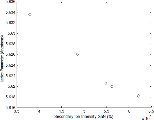
We have observed that the relation between lattice parameter and nitrogen concentration in GaNAs films is not linear for nitrogen concentration above 2.9 mol % GaN (see Figure 3). This indicates that at high nitrogen concentration, some nitrogen is being incorporated on other locations than the group V lattice sites. The fact that nitrogen is such a small atom compared to gallium and arsenic makes this incorporation on other sites than the group V lattice sites more likely.

Figure 3. Lattice parameter of different GaNAs films as function of nitrogen concentration The lattice parameter of the films was determined using HRXRD in a Philips Materials Research Diffractometer. The nitrogen concentration was measured by SIMS in an CAMECA IMS 4.5f instrument.
XPS analysis was done to confirm this hypothesis. The N(1s) spectrum for a GaN0.06As0.94 film covered with GaAs cap (see Figure 4) indicates that the nitrogen exists in two configurations: a Ga-N bond and another nitrogen-complex in which N is less strongly bonded to Ga atoms. As the GaNAs layer is buried, surface contamination should have no influence on the shape of the nitrogen peak. Rapid thermal annealing (30 seconds at 775°C) removes this nitrogen complex but also results in out-diffusion of the nitrogen.

Figure 4. XPS signal from N(1s) peak from an annealed and an not annealed GaN0.06As0.94 film measured in an PHI 5800 instrument. The Gallium Auger peak around 398 eV was removed by dividing the obtained spectrum by the spectrum of a GaAs reference sample. Annealing was done for 30 seconds at 775°C in an AG heatpulse 310.
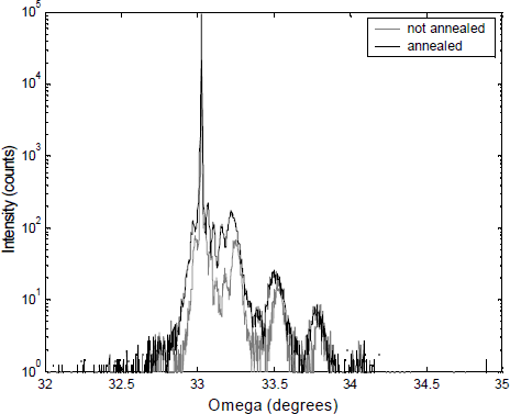
Rapid thermal annealing and the resulting disappearance of this nitrogen complex also improves of the crystal quality of GaN0.05As0.95 quantum wells as indicated by the increased X-ray intensity diffracted from an annealed 6 period 70 Å GaN0.05As0.95/130 Å GaAs superlattice (see Figure 5). The out-diffusion of the nitrogen is responsible for the slight shift of the peaks.

Figure 5. HRXRD rocking curve from an annealed and not annealed 6 period 70 Å GaN0.05As0.95/130 Å GaAs superlattice. Annealing was done for 10 seconds at 775°C in an AG heatpulse 310.
Conclusion
Growth of Nitride-Arsenides was performed by MBE using an rf plasma to generate atomic nitrogen. We have demonstrated that the nitrogen concentration can be controlled accurately by the group III growth rate as the nitrogen concentration is inversely proportional to the group III growth rate. Nitrogen exists in two binding configurations in as grown Nitride-Arsenides. We have investigated the effect of anneal on crystal quality and nitrogen binding configuration using HRXRD and XPS.
Acknowledgements
This research was supported by DARPA and ARO through contract DAAG55-98-1-0437.
The authors would like to thank Drs. P. Van Lierde and T. Schuerlein from Charles Evans and Associates for the SIMS and XPS measurements. They would also like to thank the Center for Materials Research at Stanford University and in particular B. Jones and H. Kirby for the use of the electron microprobe and the Phillips MRD.