Introduction
GaN and III-V nitride layers have been extensively investigated, since the realisation of short wavelength light emitting diodes (LEDs) and laser diodes (LDs)[Reference Nakamura, Mukai and Senoh1,Reference Nakamura, Senoh, Iwasa, Yamada, Matsushita, Kiyoku and Sugimoto2] and the demonstration of metal-semiconductor field effect transistors (MESFETs)[Reference Khan, Kuznia, Bhattarai and Olson3] and heterojunction bipolar transistors (HBTs).[Reference Pankove, Chang, Lee, Molnar, Mustakas and Van Zeghbroeck4] Low resistance and thermally stable ohmic contacts are crucial for improving such device performance. However, there are some obstacles, such as difficulty in increasing p-GaN near-surface carrier concentrations and the absence of metals having work function larger than that of p-GaN (sum of bandgap of 3.4 eV and electron affinity of 3.3 eV),[Reference Bermudez5] which make it difficult to achieve low resistance ohmic contacts to p-GaN. Jang et al.[Reference Jang, Park, Jang, Kim and Park6] investigating ohmic contacts to p-GaN using Ni/Pt/Au metallisation schemes, showed that the metal contact was ohmic with a contact resistance of 2.1×10⁻² Ωcm2 when annealed at 500 °C for 30 s in a flowing Ar atmosphere. Mori et al.,[Reference Mori, Kozawa, Ohwaki, Taga, Nagai, Yamasaki, Asami, Shibata and Koike7] investigating ohmic contacts on p-GaN using Pt, Ni, Au, and Ti single layers, showed that the as-deposited Pt contact was ohmic with a specific contact resistance of 1.3×10⁻² Ωcm2. Cao et al.,[Reference Cao, Pearton, Ren and Lothian8] investigating thermal stability of W and WSix contacts on p-GaN, reported a specific contact resistance of ∼10−2 Ωcm2 for the 300 °C annealed WSix.
To achieve low resistance ohmic contacts to p-GaN, surface treatments using the solutions of KOH and HNO3:HCl (1:3) have been performed.[Reference Lee, Kim, Lee, Park and Kim9,Reference Kim, Lee, Lee, Shin, Park and Kim10] Lee et al.[Reference Lee, Kim, Lee, Park and Kim9] employed KOH to modify surface conditions and showed that for Pd/Au contacts, the surface treatment leads to a decrease in the specific contact resistance up to 7.1×10⁻³ Ωcm2. Kim et al.[Reference Kim, Lee, Lee, Shin, Park and Kim10] used HNO3:HCl (1:3) to modify surface conditions and showed that for Pd/Au ohmic contacts to p-GaN, the surface modification results in a specific contact resistance of 4.1×10⁻⁴ Ωcm2. They attributed the low resistance to the removal of a native oxide layer that inhibits hole transport from the metal to p-GaN.
In this paper, we report on the formation of low resistance Pt contacts to p-GaN by two-step surface treatment technique using buffered oxide etch (BOE) and ammonium sulfide [(NH4)2Sx]. It is shown that specific contact resistances and Schottky barrier heights depend sensitively on the surface-treated conditions. In addition, the electronic transport mechanisms for the surface-treated Pt contacts are described and discussed.
Experimental Procedure
Metalorganic chemical vapor deposition (Emcore DGaN125™) was used to grow 1-μm-thick p-GaN:Mg (n a = 1.5-3×1017 cm−3) on (0001) sapphire substrates. The GaN layer was ultrasonically degreased in trichloroethylene, acetone, methanol, and ethanol, and rinsed in deionised (DI) water for 5 min. Prior to the fabrication of TLM patterns, mesa structures were patterned by inductively coupled plasma etching (Oxford Plasma 100) using Cl2/Ar/H2. The first-step surface treatment was performed after the mesa etching process. The mesa-patterned layers were chemically treated by three different conditions: (i) not-treated (termed here ‘A-treated’); (ii) ultrasonically boiled in BOE solution for 10 min (‘B’); (iii) first ultrasonically boiled in BOE for 10 min and then boiled in (NH4)2Sx for 10 min (‘C’). After the first-step treatment, TLM patterns were defined by photolithographic technique. The size of the pads was 100×200 μm2 and the spacing between the pads was 5, 10, 15, 20, 25, and 35 μm. After the TLM patterning, the second-step treatment was performed. All the TLM-patterned layers were dipped into BOE for 30 s. Metallisation patterns were defined using lift-off technique. The samples were then rinsed in DI water, blown dry by N2, and immediately loaded into an electron beam evaporation chamber (PLS 500). The thickness of the Pt films was 25 nm. Current-voltage (I-V) data were measured at room temperature using a parameter analyzer (HP 4155A) and Schottky barrier heights (SBHs, ϕb) were calculated using the I-V method. Electronic transport mechanisms were investigated by I-V-T data. X-ray photoemission spectroscopy (XPS) and Auger electron spectroscopy (AES) were used to investigate the variously treated surfaces of p-GaN.
Results and Discussion
Figure 1 shows the I-V characteristics of Pt contacts on the various surface-treated p-GaN. The A-treated Pt contact reveals nonlinear I-V behaviour. However, the B-and C-treated contacts show near linear and linear characteristics, respectively. Specific contact resistances (Rsc) were determined from a plot of the measured resistances versus the spacings between the TLM pads. The least square method was used to fit a straight line to the experimental data. Rsc was determined to be 3.1 (±1.1×10⁻² for the A-treated sample, 2.2 (±1.6×10⁻³ for the B-treated sample, and 3.0 (±3.8)×10−5 Ωcm2 for the C-treated sample. It is noteworthy that the C-treatment results in a dramatic reduction (by about three orders of magnitude) in Rsc as compared to that of the A-treatment. The result of the A-treated sample is comparable to that reported by Mori et al.[Reference Mori, Kozawa, Ohwaki, Taga, Nagai, Yamasaki, Asami, Shibata and Koike7]

Figure 1. I-V characteristics of the variously surface-treated Pt contacts on p-GaN.
In order to investigate the electronic transport mechanisms, the effective SBHs and the relation between Rsc and temperature were calculated by the I-V and I-V-T measurements, respectively. The I-V relation is given by [Reference Rhoderick and Williams11]

The value of A** was calculated to be 104 A cm−2 k−2 assuming the effective hole mass (mh*) of 0.8 me for p-GaN.[Reference Pankove, Bloom and Harbeke12] It is known that the measured SBHs (ϕb) are not significantly affected by the variation of A**.[Reference Sheu, Su, Chi, Jou and Chang13] Thus, the value of 104 A cm−2 k−2 was used for A** to calculate SBHs. The effective SBHs were determined at zero voltage as shown in Fig. 2. The SBH was 0.49 (±0.01) eV for the A-treatment, 0.46 (±0.01) eV for the B-treatment, and 0.43 (±0.015) eV for the C-treatment. This indicates that the reduction of Rsc can be attributed to the decrease in the SBHs.

Figure 2. Plot of I/[1-exp(-qV/kT)] vs V for the variously surface-treated samples.
According to the electronic transport theory on metal-semiconductor contacts,[Reference Rhoderick and Williams11] in principal, there are three mechanisms: thermionic emission (TE), thermionic field emission (TFE), and field emission (FE), which dominate the carrier flow. Relation between Rsc, Eoo, and SBH can be given by
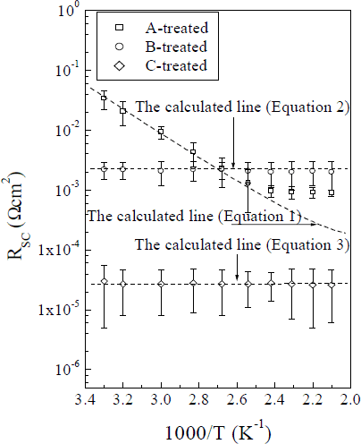
The temperature dependence of Rsc was obtained using the equations (1) − (4). (In these calculations, the SBHs and carrier concentrations of the contacts obtained by the I-V and Hall measurements were used as initial values.) Detailed results about the depth dependence of the effective carrier concentrations and the temperature dependence of tunneling parameters and effective SBHs will be published elsewhere.[Reference Jang and Seong14] Figure 3 shows the relation between Rsc and temperature. The dotted lines indicate the values that are theoretically calculated using the equations (1) − (4). For the A-treated sample, the measured specific contact resistance decreases with increasing temperature. This is in agreement with the calculated result, indicating that the dominant transport mechanism is TE. For the B- and C-treated samples, however, Rsc remains virtually unchanged over the given temperatures. The experimental results are consistent with those calculated using the approximation equations (2) and (3). This shows that TFE is dominant in the B-treated sample, whereas FE dominates in the C-treated sample. Furthermore, the SBHs of the B- and C-samples were calculated from the theoretical I-V characteristics for TFE and FE.[Reference Yu15] The calculations showed that the SBH is 0.46 eV for the B-treatment and 0.42 eV for the C-treatment. It is noteworthy that these values are comparable to those obtained by the I-V method for TE.

Figure 3. Plot of Rsc vs temperature for the various surface-treated samples using I-V-T measurements.
XPS and AES were employed to investigate the variously treated surfaces of p-GaN. Figure 4 (a) shows that the intensity of oxygen peak (O1s) varies with surface-treated conditions. This is consistent with the results of AES spectra, as shown in Fig. 4(b). It is noteworthy that no changes in the Ga 2p and the N1s peaks were observed (not shown). According to the metal-semiconductor band theory,[Reference Rhoderick and Williams11,Reference Hattori and Izumi16] the effective SBHs can be influenced by the presence of an oxide layer (with a thickness of δ) at the Pt/p-GaN interface.

Figure 4. (a) XPS and (b) AES spectra of oxygen for the various surface-treated samples (A, B and C). Comparison clearly shows that native oxide on the C-treated sample is more effectively removed than the others.
where χ is the mean tunneling barrier for carrier injection from metal to p-GaN and m is the mean tunneling effective mass of carriers. This indicates that the removal of native oxide can contribute to the reduction of the SBHs of the surface-treated contacts. Thus, the complete removal of a native oxide layer with a thickness of ∼2.5 nm is expected to result in reduction in Rsc by a factor of 15 − 18.
Based upon the results obtained using the I-V, I-V-T, XPS and AES measurements, the ohmic behaviour of the surface-treated contacts could be explained as follows. First, the reduction in the contact resistance can be attributed to the effective removal of the native oxide on the surface.[Reference Kim, Lee, Lee, Shin, Park and Kim10] Second, the surface treatments could result in an increase in the carrier concentration near the surface of the p-GaN layers.[Reference Jang and Seong14] In this work, Hall measurements were made of the A- and C-treated GaN layers before the metal deposition. Indeed, it was shown that the C-treatment leads to an increase (by about a factor of 10) in the carrier concentration as compared to the A-treatment. This is indicative of the contact systems that may consist of metal/p +-GaN /p-GaN structures for the B- and C-treated samples, making it possible for carriers to tunnel through the barriers. Third, the improvement in the contact resistance may be associated with an increase in the contact area between the metal and the p-GaN layer,[Reference Jang, Chang, Kim, Seong, Lee and Park17,Reference Jang, Park and Seong18] since the surface treatment may cause the roughening of the layer surface. Therefore, we suggest that the improvement in the specific contact resistances of the surface-treated contacts could be due to either the removal of the native oxide, an increase in the carrier concentration, an increase in the contact area, or their combined effects.
Summary
The effect of the surface treatment on the ohmic behaviour of the Pt contacts to p-GaN:Mg (1.5∼3×1017 cm−3) was investigated. Prior to the metal deposition, the two-step surface treatment was performed to modify the surface structures of the p-GaN layers: first, the layers were treated using boiled BOE and (NH4)2Sx solutions; second, all the layers were then dipped into BOE. The measurements showed that specific contact resistance was highly sensitive to the surface-treated conditions. The A-treated sample produced 3.1 (±1.1)×10−2 Ωcm2, while the BOE/(NH4)2Sx-treated contact yielded 3.0 (±3.8)×10−5 Ωcm2. Ohmic behaviour could be due to the effective removal of native oxide on p-GaN, the increase in carrier concentration at near surface, and the increase in the contact area.
Acknowledgements
This work was supported by Korea Ministry of Information and Communications (C1-98-0929) and Critical Technology 21 (Development of Power Semiconductors) (98-N5-01-01-A-08).