Introduction
There is a strong interest in GaN-based electronics for high power, high temperature applications in communications, power switching and microwave amplifiers [Reference Zolper1-Reference Wetzel and Moore9]. There have been impressive reports of high performance GaN/AlGaN heterostructure field effect transistors [Reference Binari, Redwing, Kelner and Kruppa2-Reference Wetzel and Moore9] grown on Al2O3 or SiC substrates. Other prototype devices include a depletion-mode GaN MOSFET [Reference Ren, Hong, Chu, Marcus, Schurman, Baca, Pearton and Abernathy10], GaN/AlGaN heterostructure bipolar transistors [Reference Ren, Abernathy, Van Hove, Chow, Hickman, Klaasen, Kopf, Cho, Jung, Laroche, Wilson, Han, Shul, Baca and Pearton11-Reference Han, Baca, Shul, Willison, Zhang, Ren, Zhang, Dang, Donovan, Cao, Cho, Jung, Abernathy, Pearton and Wilson13] and GaN rectifiers [Reference Bandic, Bridger, Piquette, McGill, Vaudo, Phanse and Redwing14] and junction field effect transistors [Reference Zolper, Shul, Baca, Pearton, Wilson and Shul15]. Precise pattern transfer during fabrication of these devices requires use of dry etching methods with relatively high ion energy in order to break the strong Ga-N bonds (8.92eV/atom) [Reference Shul and Pearton16]. Under those conditions there will generally be some ion-induced damage remaining in the GaN after dry etching, along with the possibility of a non-stoichiometric near–surface region due to preferential loss of atomic nitrogen in the form of N2 [Reference Ping, Schmitz, Adesida, Khan, Chen and Yang17-Reference Gillis, Choutov, Martin, Bremser and Davis19]. The Ga etch product in Cl2-based discharges is GaCl3, and this is less volatile than N2 both from a pure chemical vapor presence and from a preferential sputtering viewpoint.
There is a clear need to better understand the role of plasma exposure on the resultant electrical performance of GaN-based devices, both from an etching and deposition viewpoint. Exposure to pure Ar discharges was found to produce higher reverse bias leakage currents in p-n junction structures compared to use of Ar/N2 discharges [Reference Usikov, Lundin, Ushakov, Pushnyi, Schmidt, Zadiranov and Shuhtra20]. Even relatively low power reactive ion etching (RIE) conditions were found to deteriorate the quality of Schottky contacts deposited on plasma-etched n-GaN [Reference Ping, Chen, Yang, Khan and Adesida21, Reference Chen, Pan and Chi22]. The preferential loss of nitrogen from the GaN surface does improve the specific contact resistance of n-type ohmic contacts because of the creation of a degenerately doped surface layer [Reference Fan, Mohammad, Kim, Aktas, Botchkarev and Morkoc23].
In this work we have examined the effect of Inductively Coupled Plasma (ICP) on the reverse breakdown voltage (VB), Schottky barrier height (ϕB) and forward turn-on voltage of (VF) of GaN diode rectifiers with the contacts already in place. Several methods for damage removal were investigated, including annealing, UV ozone oxidation/stripping or wet etching with NaOH solutions.
Experimental
The diodes were fabricated on nominally undoped (n∼1017cm-3) or Si-doped (5×1017 cm−3) GaN layers ∼3μm thick grown on an n+(1018 cm−3) GaN buffer on c-plane Al2O3 substrate. Ohmic contacts were formed with lift-off Ti/Au subsequently annealed at 600 °C, followed by evaporation of the 250 μm diameter Pt(250Å)/Au(1500Å) Schottky contacts through a stencil mask. A schematic is shown in Figure 1. The samples were briefly exposed (∼10secs controlled by the system software) to 10Cl2/5Ar (total gas load 15 standard cubic centimeters per minute) or 15Ar ICP discharges in a Plasma Therm 790 reactor. During the ignition stage of discharge, the dc self-bias takes ∼2secs to reach its final value. Longer exposure time resulted in more damage. Damage layer thickness was limited due to Cl2/Ar etching of damaged GaN at a rate of around 1000 Å/min. From limited measurements we found that damage depth saturates in 10secs (∼500Å). The gases were injected directly into the source through electronic mass flow controllers, and the 2MHz source power was varied from 100-1000 W. The samples were placed on an rf-powered (13.56MHz, 5-300W), He backside-cooled chuck. Process pressure was held constant at 2 m Torr.

Figure 1. Schematic of the planar diodes
Results and Discussion
The dependence of VB and ϕB on rf chuck power for 300W source power discharges is shown in the upper part of Figure 2. Both of these parameters, at least initially, decrease with increasing power. The ϕB values saturate beyond 50W. The main effect on ϕB is from damage created around the contact periphery. This would expected to saturate once a N2-deficient region is created because much of the resultant ϕB is still determined by the unexposed region under the contact metal. Under these conditions, the dc chuck self-bias increases from − 105 V at 50 W to −275 V at 200 W. The average ion energy is roughly the sum of this voltage plus the plasma potential which is 20-25 V in this system under these conditions. After plasma exposure, the diode ideality factor was always ≥2 (the reference ideality factor was ∼1.3), which is a further indication of the degradation in electrical properties of the structures. The results are consistent with creation of an ion damaged, non-stoichiometric GaN surface region. This region exists in the plasma-exposed area outside the metal contacts. Note that the GaN etch rate increases monotonically with rf chuck power (lower part of the Figure 2), but this more rapid removal of material is not enough to offset the greater amount of damage caused by the higher-energy ion bombardment. We believe the GaN must be non-stoichiometric and hence more n-type at the surface because of the sharp decreases observed in VB. In the case of compound semiconductors with less bond energy the damage may induce into the bulk materials and the defect may traps the carriers. For GaAs where ion bombardment creates more resistive material by introduction of deep compensating levels rather than shallow donor states, the breakdown voltage is generally found to increase with exposure to plasmas.
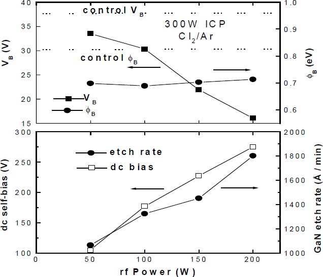
Figure 2. rf chuck power dependence of VB and ϕB in Cl2/Ar plasma exposed GaN diodes (top) and of dc chuck self-bias and GaN etch rate under the same conditions (bottom).
The dependence of VB and ϕB on ICP source power is shown in Figure 3 (top). While ϕB continues to decrease as the ion flux increases, VB initially degrades but shows less of a decrease at higher source powers. This is most likely a result of the continued decrease in the self-bias at higher source power. This also leads to a decrease in GaN etch rate above 500 W. The results of Figure 2 and 3 show that both ion energy and ion flux are important in determining not only the GaN etch rate, but also the amount of residual damage in the diodes.

Figure 3 ICP power dependence of VB and ϕB in Cl2/Ar plasma exposed GaN diodes (top) and of dc chuck self-bias and GaN etch rate under the same conditions (bottom).
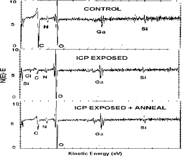
To establish the chemical state of the GaN surface at different stages, AES was performed on an unmetallized sample. Figure 4 shows surface scans before (top) and after (lower) exposure to a 500 W source power, 50 W chuck power Cl2/Ar discharge.

Figure 4. AES surface scans from GaN (top) or after (center) Cl2/Ar plasma exposure, and subsequent annealing at 700 cC for 60 seconds (bottom).
The main change is a reduction in the N2 signal in the latter sample (by ∼20%), confirming the preferential loss of this element during dry etching. Subsequent annealing at 700 °C in N2 restored some of this deficiency (Figure 4, bottom).
We also examined the use of wet etch removal of the damaged region with hot NaOH solutions (0.1M, 80 °C). This was found to be successful in etching the damaged GaN and was self-limiting in that once the undamaged material was reached, the etching stopped. We typically found a damage depth of ∼500Å. The wet etching usually can restore >70% of the original VB. The use of UV ozone oxidation followed by stripping of the oxide also produced some improvement in diode characteristics (typically ∼50% of the original VB was restored), but each cycle removes only ∼30Å, and thus 15-20 cycles would be needed to completely restore the initial properties.
Summary and Conclusions
We found that ICP Cl2/Ar discharges degrade the performance of GaN Schottky diodes, with ion energy and ion flux both playing important roles. The degradation mechanism appears to be creation of a conducting, non-stoichiometric (N2-deficient) near-surface region on the GaN. While UV ozone oxidation of the surface and subsequent dissolution of the oxidized region in HCl provides some restoration of the electrical properties of the GaN, etching in NaOH or annealing at 700 − 750 °C may restore most of the initial reverse breakdown voltage characteristics.
Acknowledgements
The work at UF is partially supported by a DARPA/EPRI grant, no. MDA 972-98-1-0006 (D. Radack and J. Melcher) monitored by ONR (J. C. Zolper), and a NSF grant DMR 97-32865 (L. D. Hess). Sandia is a multiprogram laboratory operated by Sandia Corporation, a Lockheed-Martin company, for the US Department of Energy under contract no.DEAC04-94-AL-85000.