Introduction
Heterostructures of AlGaN and GaN are being extensively investigated and employed in the fabrication of high electron mobility transistors (HEMT) and heterojunction bipolar transistors (HBT) for high-frequency and high-power applications including microwave amplifiers and compact and efficient power supplies. Prior HEMT research has confirmed the existence of a two-dimensional electron gas (2DEG) at the AlGaN/GaN heterointerface [Reference Bykhovski, Gelmont and Shur1]. Strong piezoelectric effects induce a 2D-gas at the AlGaN/GaN interface without doping. Electron sheet concentrations as high as 3×1013 cm−2 have been reported [Reference Asbeck, Yu, Lau, Sullivan, VanHove and Redwing2], [Reference Yu, Sullivan, Asbeck, Wang, Qiao and Lau3].
The development of GaN-based HBTs has received recent attention for high power/switching devices. The intrinsic high breakdown electric field of GaN should permit a GaN collector drift region that can be either much thinner and/or doped much higher relative to other semiconductors with smaller breakdown strengths (about a factor 30 compared to Si) [Reference Morkoc, Cingolani, Lambrecht, Gil, Jiang, Lin, Pavlidis and Shenai4]. Recent reports regarding the electrical properties of GaN/AlGaN HBTs indicate that the resistance in the extrinsic base region is too high to obtain satisfactory common-emitter characteristics [Reference Han, Baca, Shul, Willison, Zhang, Ren, Zhang, Dang, Donovan, Cao, Cho, Jung, Abernathy, Pearton and Wilson5]. It is desirable to have a p-type base region and the development of nitride-based HBTs centers on developing a more conductive base layer.
Acceptor-type doping of GaN materials has been problematic due in large part to passivation of Mg dopants by H. It has been established that H enhances the incorporation of dopants such as Mg, but the Mg-H bonds must be broken by post-growth annealing to achieve activation [Reference Nakamura, Mukai and Senoh6], [Reference Reboredo and Pantelides7]. However, the large piezoelectric effects from AlGaN/GaN heterostructures can potentially contribute significant conductivity in the base material relative to conventional Mg-doping.
This paper examines the extent of piezoelectric acceptor doping and modulation doping and compares these results with conventional Mg acceptor doping in AlGaN/GaN system. Material characterization including the Mg concentration profile and AlGaN/GaN interface, as determined by secondary electron mass spectrometry (SIMS), are discussed in relation to the sheet conductivity of the films.
Experimental Procedure
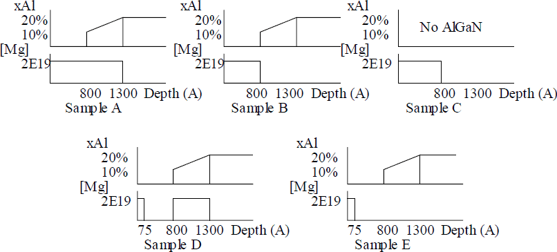
Each heterostructure consisted of a GaN (0001) film grown at 1000°C on an AlxGa1−xN (0001) layer. The latter was deposited at 1020°C on an AlN (0001) buffer layer previously deposited at 1100°C on an on-axis 6H-SiC (0001) substrate. Figure 1 shows the doping and Al profiles of the GaN and AlxGa1−xN layers in selected samples.

Figure 1. Doping and Al profiles in selected GaN/AlxGa1−xN heterostructures. The zero point of the depth scale is the top of the GaN layer.
The AlN buffer layer and all subsequent films were grown in a cold-wall, vertical, pancake-style, RF inductively heated metalorganic vapor phase epitaxy (MOVPE) system. Ammonia (NH3), triethylaluminum (TEA) and triethylgallium (TEG) were used as precursors. Bis-cyclopentadienyl-magnesium (Cp2Mg) was employed for the p-type doping. High-purity H2 was used as both the carrier and the diluent gas. After cooling to room temperature the samples were annealed at 800°C in N2 to activate the Mg acceptors. Additional details of the growth experiments in the NCSU reactor have been previously reported [Reference Weeks, Bremser, Alley and Carlson8].
Sample A contains all doping contributions: piezoelectric (PZ), modulation doping (MD) and conventional acceptors (ACC). Sample B lacks the modulation doping component. Sample C is an Mg-doped GaN film and is the control sample. It has no PZ charge or modulation doping. Sample D has doping from MD and PZ. Sample E has only PZ doping.
The Mg concentration profiles and the Al concentrations were determined using Secondary Ion Mass Spectrometry (Cameca IMS-6f) having a 100nA 10keV O2 + primary beam. Sputtering rates and Mg sensitivity factors for varying Al concentrations have been previously determined [Reference Griffis, Loesing, Ricks, Bremser and Davis9]. Analysis of the AlGaN/GaN interface was conducted by comparing the Al and Ga signals. Electrical measurements of the films were conducted using CV and Hall measurements (van der Pauw configuration). The Au(400A)/Ni(600A) ohmic contacts were produced by evaporization of the individual metals and subsequently alloying at 650°C for 20 minutes. The sheet resistance and the Hall mobility were determined for each layer.
Results and Discussion
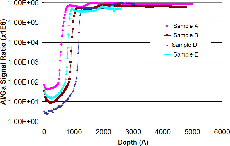
Magnesium depth profiles determined in Samples A-E are shown in Figure 2. The Mg concentration in the GaN and the Al0.1Ga0.9N layers ∼ 2×10¹⁹ atoms/cm3. A difficulty with Mg doping is the memory effect in the reactor due to the adsorption of the metal-organic precursor [Reference Ohba and Hatano10]. This leads to slightly higher conductivity from Sample D than expected from a more ideal profile, but does not affect the analysis significantly. The contribution of the polarization to the effective doping contains both a part associated with spontaneous polarization, and a part associated with strain (piezoelectric contribution). The abruptness of the interface affects the distribution of the effective charge (although not its total magnitude, provided there is no lattice relaxation). A total polarization charge as high as ps∼1×1013 cm−2 is expected at an Al0.25Ga0.75N/GaN interface [Reference Yu, Sullivan, Asbeck, Wang, Qiao and Lau3]. The sharpness of the AlGaN/GaN interface in samples investigated in this research is revealed in the SIMS plots of the Al/Ga signal ratio as a function of film depth. The AlGaN/GaN interface composition varies within a thickness of 300Å.

Figure 2. Mg Depth profiles for Samples A-E

Figure 3. AlGaN/GaN interface
The sheet conductivities of the films with the various doping contributions are presented in Figure 4. The conductivity of Sample E could not be measured.

Figure 4. Sheet conductance for Samples A-D.
All samples were more conductive than the Mg-doped GaN standard (Sample C). As all samples contained essentially equal Mg concentrations, as shown in Figure 3, the electrical data indicate that interfacial strain and modulated doping were effective in increasing the conductivity of the base material. The magnitude of the observed conductivity increase is in good accord with what would be expected on the basis of estimated polarization and modulation doping effects. For example, an added hole density of the order of 1×1013 cm−2, with a mobility of 10 cm2/Vsec, would provide an extra component of conductivity of 16 uS.
In our experiments, the GaN layer thicknesses and dopings were chosen to be of the same order as those that could be used in the base layer of an HBT. The AlGaN layers could be used as the emitter layer of the HBT, provided the structure is fabricated with the collector on the wafer surface, and the emitter is grown below the base (“collector-up” device). By contrast, the HBT structures reported to date use an AlGaN emitter on the wafer surface, on top of the GaN base (“emitter-up” device). In these structures (with (0001) films, or Ga-face growth direction), the polarization doping contributions from the emitter-base AlGaN/GaN interface provide a donor-like charge, which compensates the Mg-doping contribution, rather than adding to it.
Conclusions
Acceptor (Mg)-doped AlxGa1−xN/GaN heterostructures and a similarly doped GaN standard layer have been grown via MOVPE and the sheet conductance determined from CV measurements. Secondary ion mass spectroscopy shows Mg concentrations in the films of ∼2×1019 cm−3. The Mg concentration in all the films was essentially uniform; however, each film possessed a different conductivity depending on the presence and the magnitude of piezoelectric charges and the modulated doping. Additionally SIMS analysis of each film showed a sharp AlGaN/GaN interface (∼300 Å) that enhances both the interfacial strain and the piezoelectric charge. Sheet conductance measurements showed that all AlxGa1−xN/GaN heterostructures exhibited greater conductivity than the pure GaN sample. This strongly indicates that piezoelectric doping and modulated doping increase the base material conductivity over that achieved by conventional acceptor doping.
Acknowledgements
The authors acknowledge Cree Research, Inc. for the SiC wafers. This work is supported by the Office of Naval Research under contracts N0W14-98-1-0654 (John Zolper, monitor).