Introduction
The lack of GaN substrates limits the performance of GaN-based devices including light emitters and microwave power transistors. No doubts, only GaN itself can meet the requirements on perfect substrates for advanced GaN-based electronics.
Recently, we have demonstrated that high quality bulk GaN single crystals can be grown from the liquid phase at reasonably low temperatures (<1100°C) and pressures (<2 atm) [Reference Ivantsov, Sukhoveyev and Dmitriev1]. The crystals were grown via spontaneous nucleation on the melt surface. It was found that crystals possessed so fine optical properties that for the first time room temperature stimulated emission was registered from the bulk GaN material. Measured in wide temperature range, optical bandgap of these crystals was occurred closer to that of epitaxial material than to bandgap of bulk GaN grown at high pressure [Reference Sukhoveyev, Ivantsov, Zubrilov, Nikolaev, Nikitina, Bougrov, Dmitriev and Tsvetkov2, Reference Teisseyere, Perlin, Suski, Grzegory, Porowski, Jun, Pietraszko and Moustakas3]. In this paper, we present recently obtained results on the seeded growth from the liquid phase of GaN boules.
Experimental Equipment and Procedure
Growth experiments were conducted in a vertical 300-mm diameter water-cooled chamber. The chamber was made of stainless steel and equipped with viewing and vacuum ports. Quartz viewports gave a chance of in situ observation of the growing crystal during the growth run. A 5 MHz rf-generator supplied up to 10 kW power for heating of a graphite susceptor. Linear and rotation motion of the seed was activated using manual and/or motorized actuators.
Prior to the growth run, the hot zone was degassed at 1100°C down to 10−5 Torr residual pressure. Then, charge materials were put in a graphite crucible and chamber was evacuated as soon as possible to reduce an inevitable contamination of the growth zone from the atmosphere. After the evacuation, the chamber was filled with nitrogen-rich gas mixture at a total pressure not exceeding 2 atm. Meanwhile, temperature of the heater was rised to a growth temperature chosen from 850-1000°C range. The started temperature was maintained constant for the launch period within an accuracy of ±0.5°C and decreased after that down to 800°C by the end of the growth run. Growth run lasted no longer than 10 hours.
The growth of GaN boule was initiated on the graphite rod that was used as a seed. Normal growth rate was piloted by the velocity of seed linear motion that was settled at about 2 μm/hr. As a result of the growth experiments, GaN ingots up to 21 mm in diameter and 15 mm in length were grown (figure 1). The ingots were sliced in approximately 2 mm thick wafers. In order to evaluate these wafers, homoepitaxial GaN layers were grown by hydride vapor phase epitaxy (HVPE).

Figure 1. As-grown ∼20-mm diameter 15-mm in length GaN ingot (a). The same ingot after etching in HF+HNO3 mixture and sawing in ∼2 mm thick wafers (b).
The composition analysis of the wafers was carried out in scanning Auger electron spectroscopy–secondary ion mass-spectrometry (AES-SIMS) homemade analytical setup with the minimum back pressure of 10−11 Torr. For the SIMS measurements, secondary ion complexes are mass-filtered and focused by an objective system, which allows independent adjustment of ion beam diameter and density. The area of scanning zone is 500×500 μm2 and ion current ranges from 0.2 to 20 mA/cm2. High transmission secondary ions optics with a narrow-band pass energy provides mass resolution of the quadruple filter (3M) with a dynamic range of six orders of magnitude. It is a main feature of the setup that, due to the weak draw field of secondary ions, simultaneous AES and SIMS analysis are possible. For the AES measurements, cylindrical mirror analyzers with energy resolution of 0.5 % and a coaxial electron gun with an energy of 3 keV and an electron beam size of 5 µm were used. Electron beam is matched with the center of the crater being ion etched. The specific procedure of surface cleaning during the measurements was developed to reduce oxygen reabsorption effect. Monitoring the signals of GaLMM and NKLL transitions at 1066 eV and 376 eV, respectively, the composition of bulk GaN was measured.
To characterize the structure of the ingots and HVPE grown homoepitaxial layers, x-ray diffraction (XRD) measurements were done in ω -2θ scanning geometry. As a reference crystal in double-axis XRD setup, high quality Lely 6H-SiC crystal with lattice parameters of a=3.0817 Å and c=15.1183 Å was used.
Room temperature micro-cathodoluminescence (micro-CL or SEM-CL) measurements in scanning electron microscope (SEM) were employed together with routine CL measurements at ∼90 K for optical characterization of GaN wafers and epilayers. The SEM-CL study was conducted at electron beam current of 10−8 A and beam diameter of 1000 Å.
Results
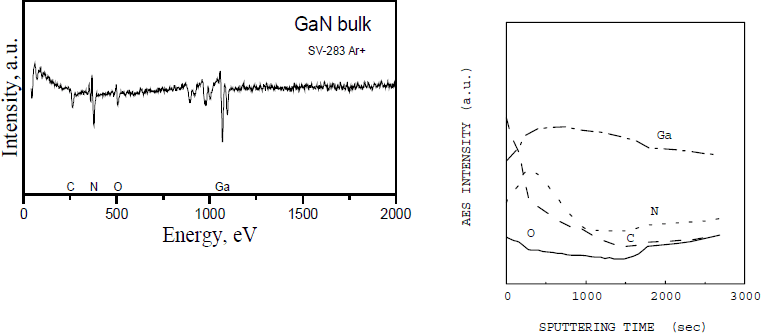
Several GaN ingots having the diameters from 16 to 21 mm and lengths from 10 to 15 mm were successfully grown. The AES spectrum features gallium and nitrogen related peaks typical for GaN. The oxygen (OKLL at 504 eV) and carbon (CKLL at 263 eV) intense peaks were believed to appear due to the surface oxidation and contamination. Apart from carbon and oxygen, there was not any other element being detected within the limits of instrumental resolution. The sample was sputtered for 20 sec by Ar + beam in order to remove surface contamination (figure 2, left). Oxygen and carbon peaks still presented in the spectrum, but intensities of them significantly reduced. To detail the distribution of the impurities in the bulk of the crystal, a depth-profile SIMS measurements were performed (figure 2, right). The traces of oxygen and carbon, which were detected in the bulk of GaN, most probably are associated with grain boundaries, since microscopical observations made after chemical etching showed that sliced wafers are composed of separate micron-size crystallites having pyramidal and platelet shapes.

Figure 2. Auger electron spectrum (left) and secondary ion depth-profile (right) taken from the bulk GaN polycrystalline sample after Ar+-beam sputtevariation of N and Ga signals are likely due to “sputtering effect”.
Secondary electron microscopical image and SEM-CL map of GaN wafer are shown in figure 3. They showed as small as 1-3 μm size grains with the boundaries exhibiting strong signal in yellow luminescence collection mode.

Figure 3. Secondary electron microscopy image (a), and SEM cathodoluminescence map (b) of the wafer that was sliced from the GaN ingot (RT, 1000x).
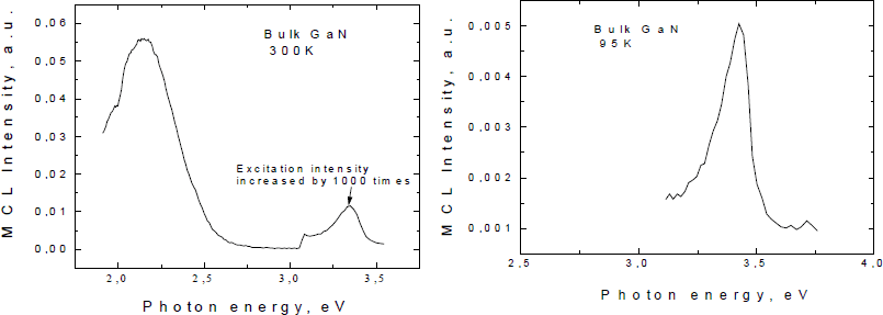
SEM-CL spectra measured at both room temperature (RT) and 95 K detected strong yellow luminescence and weak exciton-related lines (figure 4). Donor-acceptor pair recombination did not observed.

Figure 4. Cathodoluminescent spectra taken from a GaN wafer at room temperature (left) and edge CL peak measured at 95 K (right).
The XRD measurements showed the presence of (10
Figure 5. Figure 5. X-ray diffraction spectra for GaN substrate (solid line) and deposited homoepitaxial GaN layer (dash-dot line).
In order to estimate the potential of the developed technique for GaN substrate manufacturing, preliminary HVPE experiments were performed on GaN substrates, which were prepared from the grown ingots. To remove residua of the melt, the wafers were etched in HF+HNO3 mixture and cleansed in organic solvents and deionized water. The wafers were polished and lapped to finish the surface of the wafers for subsequent epitaxy. About 3-μm thick GaN layer was successfully grown using routine HVPE procedure developed for GaN epitaxy on SiC and sapphire substrates [Reference Melnik, Nikitina, Zubrilov, Sitnikova, Musikhin and Dmitriev4]. Epitaxial layer was free of cracks. Results of the XRD measurements are shown in Figure 5 (dash-dot line). It is clearly seen that (10
Conclusion
GaN ingots were grown from the Ga-based melt in the temperature range of 800-1000°C at less than 2 atm ambient pressure. Growth was performed on the graphite seed at ∼2 mm/hr growth rate. Grown ingots were sliced in ∼2 mm thick wafers, which were characterized on structural and optical properties. X-ray diffraction analysis revealed polycrystalline structure of the wafers with the [10
GaN 3 µm thick homoepitaxial layer deposited on GaN substrate fabricated from the ingot was stress-free and displayed improved structural and optical properties in comparison with the substrate.
Presented results show that large volume GaN ingots can be grown from liquid phase using seeded technique. We believe that these results open the opportunity to develop seeded technique for bulk growth of bulk GaN crystals. Future research will be directed to single crystal growth of bulk GaN from liquid phase.
Acknowledgements
The authors greatly acknowledge Dr. M. Spencer for extremely helpful discussions. The research at the CGRC and Ioffe Institute was partially funded by the Russian Fund for Fundamental Research (Project No. 97-02-18057). Work at TDI, Inc. was supported by ONR Contract N00014-99-C-0346 (Program Monitor Dr. Colin Wood).