Introduction
Magnesium is the most common acceptor used in GaN. The large activation energy of Mg of 150 meV to 250 meVReference Strite and Morkoc 1 , Reference Nakayama, Hacke, Khan, Detchprohm, Hiramatsu and Sawaki 2 , Reference Fischer, Wetzel, Haller and Meyer 3 results in a low acceptor ionization probability. Other acceptors such as Be and Ca also have large activation energies of 150 meVReference Ronning, Carlson, Thomson and Davis 4 and 169 meVReference Lee, Pearton, Zolper and Stall 5 , respectively. The low acceptor activation in p-type GaN results in large series resistances and high operating voltages, thereby adversely affecting the performance of electronic and optoelectronic devices.
Recently, it has been theoretically demonstrated that doped superlattice (SL) structuresReference Schubert, Grieshaber and Goepfert 6 increase the free hole concentration as compared to homogeneous thin-film p-type GaN. Doped superlattices are doped ternary compound semiconductor structures with a spatially modulated chemical composition. The modulation of the chemical composition leads to a variation of the valence band energy and to a reduction of the acceptor activation energy. Acceptors in the GaN layers of the superlattice must be ionized by thermal excitation. However, acceptors in the Al x Ga1−x N barriers are ionized more easily because these acceptors are close to the GaN valence band edge.
Experimental
In this publication, the electronic properties of Al x Ga1−x N/GaN doped superlattice structures grown by MBE are analyzed. The superlattices consist of 20 periods of equally thick AlxGa1−xN barriers (10 nm) and GaN wells (10 nm). The Al x Ga1−x N and GaN layers are uniformly doped with Mg at a level of NMg ≈ 1019 cm−3. The Al mole fraction of the two different doped SLs are x = 0.10 and 0.20.
Hall-effect measurements were conducted on Mg-doped Al x Ga1−x N/GaN superlattice samples. Photolithographically defined, 85 nm thick Ni contacts were deposited by electron-beam evaporation in the van der Pauw configuration. All samples display ohmic I-V characteristics. The samples were cooled in a Cryo Industries liquid nitrogen cryostat. Hall effect measurements, with a magnetic flux density of 0.5 T, were made between 150 - 400 K with 10 K intervals.
Experimental results and discussion
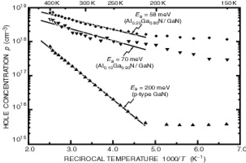
Figure 1 shows the free hole concentration verses reciprocal temperature. The hole concentration displays an exponential dependence for temperatures in the range 220 - 400 K. The natural logarithm of the carrier concentration verses reciprocal temperature is fit with a least squares regression algorithm. The activation energy is determined using the relation
where E a is the effective acceptor activation energy, k B is Boltzmann’s constant, and T is the absolute temperature. The measured activation energies for the superlattices with x = 0.10 and x = 0.20 are 58 meV and 70 meV, respectively. This result clearly shows that doped Al x Ga1−x N/GaN superlattice structures have a lower activation energy than homogeneous Mg-doped GaN thin films.

Fig. 1. Hole concentration verses reciprocal temperature for Mg-doped Al x Ga1−x N/GaN superlattice samples with Al mole fraction in the barriers of x = 0.10 and 0.20. Also shown is a uniformly Mg-doped GaN thin-film sample with an acceptor activation energy of 200 meV.
At room temperature, the carrier concentration of the doped SL structures are 2 × 1018 cm−3 and 4 × 1018 cm−3for an Al mole fraction x = 0.10 and x = 0.20, respectively. The sample with 20 % Al shows a factor of two larger carrier concentration than the sample with 10 % Al. Clearly, the free hole concentration increases with an increase of Al mole fraction in the barriers of the doped SLs. This increase is consistent with theory. It should be noted that most free carriers reside in the GaN layers. Assuming that the carrier concentration in the barriers is much smallerReference Schubert, Grieshaber and Goepfert 6 than in the GaN well layers, the actual free carrier concentration the GaN well layers of the superlattice is 8 × 1018 cm−3 which is the highest free hole concentration ever achieved in GaN.
Katsuragawa and coworkersReference Katsuragawa, Sota, Komori, Anbe, Takeuchi, Sakai, Amano and Akasaki 7 showed that as the Al content is increased in homogeneous Al x Ga1−x N from x = 0.00 to x = 0.33 the hole concentration decreases monotonically. Tanaka and coworkersReference Tanaka, Watanabe, Amano, Kobayasi, Akasaki, Yamazaki and Koike 8 reported that for Mg-doped GaN to Al0.08GaN0.92N, the activation energy increases from 157 meV to 192 meV. In contrast, doped superlattice structures have smaller activation energies and larger carrier concentrations as the mole fraction of Al is increased in the superlattice barriers.
The conductivity verses temperature for the two SL structures are depicted in Figure 2. The room-temperature conductivity is 0.27 S/cm and 0.64 S/cm for the superlattice with an Al mole fraction of x = 0.10 and 0.20, respectively. At room temperature the conductivity for the SL with 20 % Al has a conductivity almost a factor of three greater than for the SL with 10 % Al. Note that the results shown in Figure 2 are the highest p-type conductivities achieved in a III-nitride semiconductor containing aluminum.

Fig. 2. Conductivity verses temperature for p-type Al x Ga1−x N/GaN doped superlattices and homogeneous p-type GaN.
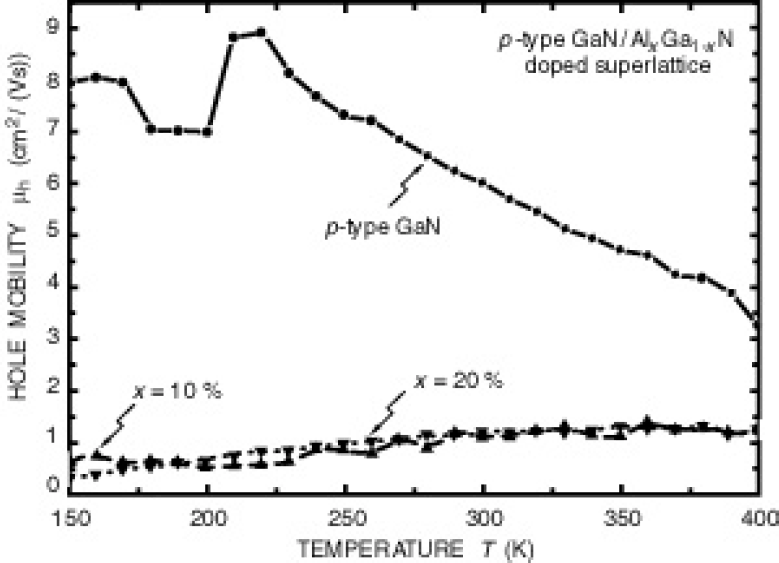
Figure 3 depicts the mobility verses temperature for the doped superlattice samples. Note, that for an increase in Al content, the mobility does not change. The mobilities of the doped SL structures increase monotonically with temperature by more than a factor of three in the temperature range 150 - 400 K. This is in contrast to p-type GaN which exhibits a decrease in mobility as the temperature increases beyond 200 K. Due to the temperature dependence of the mobility, conductivity data without carrier concentrationsReference Saxler, Mitchel, Kung and Razeghi 9 will result in an overestimation of the acceptor activation energy.

Fig. 3. Mobility verses temperature for p-type Al x Ga1−x N/GaN doped superlattices and homogeneous p-type GaN.
We have calculated the carrier concentration as a function of temperature for an Al x Ga1−x N/GaN doped superlattice with x varied between x = 0.00 and x = 0.30. The thicknesses of the GaN and Al x Ga1−x N regions are both 10 nm. A uniform doping profile of N A = 1 × 1018 cm−3 and an acceptor activation energy of E a = 200 meV in the GaN and the Al x Ga1−x N is assumed. Using the parameters εr = 9.0 − 0.5 x for the relative permittivity 10 and m p* = 0.8 m 0 for the effective hole mass 11 , the hydrogenic model does not predict a significant deepening of the acceptor level in Al x Ga1−x N for x ≤ 0.20 This is consistent with the experimental results of Katsuragawa et al.Reference Katsuragawa, Sota, Komori, Anbe, Takeuchi, Sakai, Amano and Akasaki 7 who showed that the activation energy does not change markedly with the Al content. To determine the carrier concentration, the arithmetic average of the position dependent carrier concentration over one period of the superlattice is computed for a given Al content and temperature.
Figure 4 depicts the calculated carrier concentration verses 1/T for four doped SLs with different Al content in the Al x Ga1−x N barriers. Examination of the four curves shows that the carrier concentration increases with an increase in Al content in the barriers. Note, that in the freeze-out regime, the slope of each curve represents the effective activation energy of the acceptor, which decreases with increasing Al content in the barriers. Our experimental results shown in Figure 1 are consistent with the results of the theoretical model.

Fig. 4. Calculated hole concentration verses reciprocal temperature for p-type Al x Ga1−x N/GaN doped superlattices with Al mole fractions of x = 0.00, 0.10, 0.20, and 0.30.
Conclusions
In conclusion, the electronic properties of Mg-doped superlattices consisting of uniformly doped Al x Ga1−x N and GaN layers are analyzed by Hall-effect measurements. Acceptor activation energies of 70 meV and 58 meV are reported for superlattice structures with an Al mole fraction of x = 0.10 and 0.20 in the barrier layers, respectively. These energies are substantially lower than the activation energy measured for Mg-doped GaN thin films. At room temperature, the doped superlattices have free hole concentrations of 2 × 1018 cm−3 and 4 × 1018 cm−3 for x = 0.10 and 0.20, respectively. The increase in hole concentration with Al content of the superlattice is consistent with theory. The room temperature conductivity measured for the superlattice structures are 0.27 S/cm and 0.64 S/cm for an Al mole fraction of x = 0.10 and 0.20, respectively.
The work at Boston University was supported in part by the ONR (Dr. C. E. C. Wood) and by the NSF (Dr. R. P. Khosla). The work at NZ Applied Technologies was supported by the NSF (Dr. D. Gorman).