


I. INTRODUCTION
Organic and hybrid optoelectronic devices like perovskite and organic photovoltaic cells, organic light emitting diodes (OLEDs), and the like consist of a complex stack of thin layers of functional materials. Reference Fung, Li and Liao1–Reference Kazim, Nazeeruddin, Grätzel and Ahmad3 Relatively efficient OLEDs have already been demonstrated some decades ago where the organic semiconducting layers were deposited as thin films by evaporation. Reference Tang and van Slyke4,Reference Friend, Gymer, Holmes, Burroughes, Marks, Taliani, Bradley, Dos Santos, Brédas, Lögdlund and Salaneck5 A typical OLED device architecture is shown in Fig. 1, displaying the various materials necessary for efficient charge injection and transport and light emission by radiative recombination. This is an example of the so-called bottom emissive OLED, which is built on a transparent substrate and finished with a nontransparent reflective electrode so that the generated light is emitted through the substrate. When nontransparent (e.g., metallic) substrates are used, the light is emitted directly from the device instead of through the substrate, and the so-called top emissive device is obtained. All the work presented in this study relates to bottom emissive stacks. The commercial industrial production of these devices, e.g., for the consumer electronics market, is currently dominated by vacuum based “dry” deposition techniques like sputtering and evaporation. Reference Lee6 Although these processes are well-established, device fabrication by solution processing, i.e., by printing and coating of functional inks, has emerged as a promising alternative route toward industrial mass production of organic optoelectronic devices. Reference Duggal, Heller, Shiang, Liu and Lewis7–Reference Derue, Olivier, Tondelier, Maindron, Geffroy and Ishow10 For solution processing on the academic laboratory scale, spin coating is frequently the method of choice for the thin layer deposition due to its ease of application and its good control over the layer thickness and homogeneity. Reference Derue, Olivier, Tondelier, Maindron, Geffroy and Ishow10 For industrial production, however, it suffers from its lack of compatibility with high volume manufacturing and its inefficient use of materials. Research aimed at results more directly applicable in an industrially relevant production environment therefore focuses on other techniques, like slot-die coating. Reference Peters, Wengeler, Scharfer and Schabel8,Reference Choi, Lee, Park and Seo11–Reference Raupp, Merklein, Pathak, Scharfer and Schabel14

FIG. 1. (a) A schematic cross-section of the OLED device stack used in this study. (b) A schematic cross-section of a bottom emissive OLED device with unpatterned functional layers. (c) Corresponding image for a device with patterned functional layers sandwiched between a top and bottom barrier. Water ingression via the side is only possible for (b).
This approach exhibits its own specific challenges not encountered in vacuum processing, but there are also distinct benefits associated with it, which, for certain application areas, show good prospects for replacing dry deposition technologies on the mid-term. Many of these beneficial characteristics are related to the possibility of processing at atmospheric pressure, with more efficient materials use, high throughput, and at low overall production cost. Reference Sandström and Edman15 Several recent publications have demonstrated that slot-die coating can be used for the production of highly efficient OLED devices by solution based techniques. Reference Choi, Lee, Park and Seo11–Reference Raupp, Merklein, Pathak, Scharfer and Schabel14 These studies, however, have all made use of sheet-to-sheet (S2S) processing. An especially interesting aspect of slot die coating and several other solution processing methods is production upscaling by roll-to-roll (R2R) manufacturing techniques. Reference Hast, Tuomikoski, Suhonen, Väisänen, Välimäki, Maaninen, Apilo, Alastalo and Maaninen16–Reference Søndergaard, Hösel and Krebs18 R2R slot-die coating is a common technology which has been used for a long time already for the production of photographic films and coated papers. It offers a way to apply a wet layer on a substrate in a very well controlled manner. In the field of flexible electronics, the technology is used for making the active layers in OLEDs and organic or perovskite based solar cells. Reference Hast, Tuomikoski, Suhonen, Väisänen, Välimäki, Maaninen, Apilo, Alastalo and Maaninen16–Reference Søndergaard, Hösel and Krebs18 Recently, impressive progress has been achieved in the field of organic photovoltaic (OPV) device production by the R2R solution based approach. Reference Koidis, Logothetidis, Ioakeimidis, Laskarakis and Kapnopoulos19–Reference Amb, Craig, Koldemir, Subbiah, Choudhury, Gevorgyan, Jørgensen, Krebs, So and Reynolds21 In this paper, we report on our own results regarding the R2R processing of OLED devices by wet deposition of functional inks for the hole injection and emissive layers.
II. RESULTS AND DISCUSSION
A. Tandem R2R coating line for high yield printed electronics production
Particle contamination is a serious problem in the production of organic electronic devices, a. o., because the functional layers used are rather thin (in the order of 20–200 nm), and any particles of a comparable or larger size pose a high risk for defects. A typical source for dust particles is top contact with the functional layers during processing and sample handling, e.g., by web handling parts like nips or idler rollers. When R2R fabrication techniques are applied, as is frequently the case in industrial production environments, particle contamination can also occur by contact with the backside of the substrates during rewinding. The consequence can be malfunctional devices, decreased performances, shortened lifetimes, and lower production yields. Whereas a significant percentage of deficient products can frequently be tolerated in an academic research environment, this is absolutely prohibitive for industrial manufacturing processes. A strategy to reduce the risk of particle contamination due to backside contact in R2R processes is therefore the sequential processing of several functional layers in a single run (“tandem R2R coating”), without rewinding between the coating steps. In addition to the reduced particle contamination, the related reduction in production costs is another benefit. Its disadvantage, however, is the need for extensive web handling and thus frequent risk of surface top contact. In addition to working in a cleanroom environment, a web handling system which avoids top contacting while still enabling sequential coating is therefore a prerequisite for success.
Whereas for the production of a complete organic solar cell or OLED by R2R solution processes, at least three, but more typically five or even more, sequential coating steps will be necessary, the general concept can already be demonstrated and investigated by two sequential steps carried out in tandem. A schematic drawing and photographs of the system used in this study are shown in Fig. 2, which employs a novel concept that allows the transport of the carrier substrate through two sequential coating stations and drying ovens, including several 90° and 180° turns, without ever making contact to the top surface. To save cleanroom space, only the winder, re-winder, and coating stations are located in a cleanroom environment, whereas the dryers are located outside. This separation of the process parts between cleanroom and noncleanroom areas drastically reduces the footprint of the needed cleanroom area compared to the total process area. In addition to the corresponding cost savings, this also allows relatively easy control of the cleanroom environment and particle density. Inside the ovens, the use of parts which move or touch the web on the rear side is limited to reduce sources for particle generation. Initial particle level measurements (without a moving web) showed a cleanliness level between ISO 3 and ISO 4 according to the cleanroom standard ISO 14644-1. If necessary for the drying of air-sensitive materials, the ovens can be operated under nitrogen atmosphere, with an oxygen concentration of below 80 ppm.

FIG. 2. (a) A schematic drawing of the tandem coating line comprising two subsequent coating stations in one process. (b) A schematic drawing of the web pass in the process which allows substrate handling without ever touching the top side. (c) A photograph of the cleanroom part of the line, showing the coating stations. (d) A photograph of one of the drying ovens outside the cleanroom environment.
B. Patterned deposition of functional layers from solution
In addition to their sensitivity to dust particles, the functional layers of organic electronic devices also need to be protected carefully against water and oxygen ingression, which quickly degrade many of the materials used in them. Whereas encapsulation of the top and bottom surfaces can be rather easily achieved by the use of barrier technologies, Reference van de Weijer, Bouten, Unnikrishnan, Akkerman, Michels and van Mol22 ingression via the sides is frequently a serious challenge. This is especially relevant for production processes that employ homogeneous coating techniques, with only very limited options for locally selective deposition of the functional layers, as is the case for, e.g., R2R slot-die coated OLEDs. Once a roll of finished products is ready, the individual OLED modules must be cut from it to achieve the required dimensions. As illustrated in Fig. 1(b), this will inevitably result in the unpatterned coated layer becoming exposed to the ambient environment at the cut edges, thereby opening an ingression route for moisture and oxygen. The consequence will be the immediate start of device deterioration via side leakage, unless efficient sealing at the device edges can be achieved. Any option to pattern the functional layers will significantly ease an efficient encapsulation because some noncoated regions are available next to the functional areas, where the top and bottom barriers can be brought into direct contact with each other [Fig. 1(c)].
Whereas in the case of small scale production for research purposes, especially when using sheet-to-sheet (S2S) techniques like spin coating, the partial removal of functional materials is commonly achieved by wiping, this is obviously no option in an industrial production environment. Selective removal of the dried layers by laser ablation is a more viable route, which has been demonstrated in the case of OPV cell production, Reference Galagan, Fledderus, Gorter, ’t Mannetje, Shanmugam, Mandamparambil, Bosman, Rubingh, Teunissen, Salem, de Vries, Andriessen and Groen23 but it is typically rather slow and creates debris particles, which can redeposit on the functional area and cause problems when the following layer is coated. Furthermore, prepatterning of the substrate by localized plasma treatment to induce self-assembly of the coated layers is a possible solution, Reference Svarnas, Yang, Munz, Edwards, Shard and Bradley24 but no satisfying results have been obtained up to now in the field of OLED production. The most straightforward option is therefore to pattern the functional layers directly during the coating process, i.e., to achieve locally selective deposition. This removes the need for the removal of excess material afterward in an additional processing step and also avoids the risk of contamination with debris particles.
C. R2R stripe coating
Due to its nature as a basically homogeneous deposition technology, slot-die coating, as opposed to, e.g., inkjet printing, is not suited to create complex patterns in a variety of shapes. Rather, by partially restricting the ink flow in the coating direction and opposite to it, it allows the production of simple patterns like stripes and rectangles. In many cases, however, these limited patterning options are already sufficient to prepare functional coatings that can be efficiently encapsulated to yield devices which are stable against degradation by side leakage. As the techniques to achieve patterned slot-die coating vary considerably, depending on whether patterning in or opposite to the web direction is the goal, they will in the following be treated separately.
For patterning in the coating direction, stripe coating is a rather common method. Reference Han, Lee, Ahn, Nam and Jung25 In conventional stripe coating, the ink flow through the slot-die onto the substrate is partially prevented by a shim, which is mounted into the slot gap of the device, as shown in Fig. 3(a). As the ink can exit the slot-die only at the locations where its flow is unobstructed by the presence of the shim, the result is a stripe pattern, the dimensions of which are determined by the shim geometry. This approach, however, has the disadvantage that lateral wetting on the coating lip will occur by capillary forces, leading to a loss of control over the exact width of the stripes in the pattern. The resulting value of the stripe width will be larger than defined by the shim, but the exact deviation is determined by a complex interaction of many factors and therefore inherently unpredictable. Reference de Vries and Gabel26 A solution to this problem, as implemented in the coating line described in the present study, is the use of notched dies, as is shown in Fig. 3(b). In this design, the die lips are notched in accordance with the desired stripe pattern and thus lateral spreading of the coating solution on the lips is suppressed. In this way, the deposited stripe widths correspond very closely to the value determined by the notch design, as can be seen in Fig. 3(c).

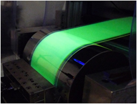
FIG. 3. Options for R2R stripe coating. (a) Slot-die with shim. (b) Notched slot-die designed for accurate stripe coating and a detail of the notched die lip (inset). (c) Well-defined stripe coating using a notched slot-die. Stripe pattern as defined in Table I, total coating width 240 mm. (d) Stripe coating of EML ink on the HIL under UV illumination.
Table I presents the results of a stripe coating study using various test fluids, one based on water and one on a nonpolar organic solvent (xylenes), with different rheological properties, at two coating speeds. The notches were prepared in such a way that patterns of stripes alternating with noncoated interspaces were produced. Three different test patterns were examined, comprising parallel stripes with 9, 8, and 7 mm design widths and a spacing of 1, 2, and 3 mm, respectively. The actual measured widths obtained using these notched dies were only slightly larger than the targeted design width, the maximum deviation being 5%. This good agreement between the designed stripe width and the experimentally obtained values indicates the virtual absence of lateral spreading due to the capillary effect.
TABLE I. Widths of spacings between stripes coated using notched slot-die lips with different designs (Agfa V109 PET film, coating gap: 100 µm, wet coated layer thickness: 10 µm, polymer concentration 10 g/L).

As can be seen in Fig. 3(d), stripe coating using notched slot dies also works with actual functional OLED materials (emissive layer [EML] on hole injection layer [HIL] in this specific case), where another test pattern with broader stripes was used. In agreement with the experiments done using the test fluids, also in this case, good agreement between target and obtained widths was observed (deviation +6%).
D. R2R intermittent coating
Whereas patterned slot-die coating in the web directions (stripe coating) is rather straightforward, patterning perpendicular to the coating direction is more complicated. In this case, the flow of the ink onto the substrate does not simply need to be confined locally. Instead, it actually must be stopped and started in a controlled manner, without causing ill-defined edges by start or stop effects. This controlled interruption of the coating process is known as intermittent slot-die coating and has been described for the production of lithium ion batteries. Reference Schmitt, Diehm, Scharfer and Schabel27 In this particular case, the thixotropic behavior of the coating slurry in combination with its relatively high viscosity enabled intermittent coating to be initiated simply by stopping and starting the ink flow. When we tried to transfer this process to the rather low viscosity coating solutions typically used in the field of the solution processing of OLED materials (1–10 mPa), the results were disappointing. Under these circumstances, the capillary forces are dominant over the shear stress in the coating bead. The result of an initial coating experiment using an ink for the HIL is displayed in Fig. 4(a). Upon starting of the coating flow, an irregular pattern with streaks was observed, which only stabilized into a uniform closed layer after several centimeters away from the starting position. Similarly, the interruption of the coating flow resulted in a gradual thinning of the coated layer, before final break-up of the trailing edges was achieved. Again, this process took several centimeters until finally no ink was deposited. Obviously, this is a situation which does not allow the reproducible production of OLED devices.

FIG. 4. R2R intermittent slot-die coating. (a) Leading coating edge and trailing coating edge for an HIL ink during conventional intermittent coating (without moving die). (b) A schematic representation of the principle of intermittent slot-die coating using a moveable die. (c) A schematic drawing of the moveable intermittent slot-die coating station. (d) Intermittent coating of a test solution using this equipment. (e) Leading coating edge and trailing coating edge for this test ink and (f) for the HIL ink during intermittent coating using the moveable intermittent slot-die station.
A much more desirable coating behaviour was obtained when, in addition to the start or stop of the ink flow, a coating unit was developed in which the entire slot-die was moved close to or away from the substrate [Figs. 4(b) and 4(c)]. In this design, the coating gap can be widened from the coating position (50–100 µm away from the web) to a maximum distance of 4 mm within 25 ms. In practice, a stoke of 1 mm turned out to be sufficient to reliably break up the coating bead and to enable well-defined coating edges. The process and its result are shown in Figs. 4(d) and 4(e), where for reasons of visibility and to demonstrate the general applicability of the method also to nonpolar formulations, a xylene-based test liquid containing a dye is used. In addition, this liquid serves as a test model for the EML ink, which itself is also a solution of the emitter polymer in xylene. The vibrations induced by the high speed mechanical motion of the slot-die were expected to be carried forward into the stream of ink onto the substrate and thus to cause regular variations perpendicular to the coating direction, known in literature as barring. Reference Kistler and Schweizer28 To compensate for the movement and to suppress these vibrations, counter balance masses, which move in the opposite direction as the retraction motion of the slot, were included in the design. In addition, the moving parts of this process are mounted on leave springs to further dampen any residual vibrations. Taken together, these measures enabled us to significantly improve the straightness and thickness homogeneity of the leading and trailing edges during intermittent slot-die coating, as is displayed in Fig. 4(f) for the HIL ink.
E. R2R coating of functional OLED layers
To arrive at a process allowing device coating under optimized conditions, the deposition procedures for each of the functional inks were studied individually first. The HIL formulation used is based on a mixture of several solvents. As a consequence, it has a low surface tension (30–31 mN/m) and thus spreads and wets well on the test substrates (pure poly(ethylene terephthalate) [PET] and poly(ethylene naphthalate) [PEN], and PET coated with indium tin oxide [ITO]) (wetting angles <10°). On the other hand, good contact line pinning is also observed, meaning that the ink reliably stays on the coated area without spreading beyond. To achieve dry HIL film thicknesses of 30 nm or 60 nm at a line speed of 5 m/min, it was found that wet films in the order of 8 µm or 16 µm, respectively, needed to be deposited. At first sight, the resulting dry coatings looked uniform by visual inspection, but as the layers are thin and highly transparent, this is difficult to qualify reliably by the unaided eye. Indeed, closer examination using contrast enhancement (by placing a white paper below the sample and increasing the HIL thickness to 90 nm) revealed a slight mottle or spottiness within the layers [Figs. 5(a)–5(d)]. Using such HILs in complete OLED devices revealed that this mottle effect in the HIL, even though hardly visible in the layer itself, had a significant influence on the homogeneity of the light output in full OLED devices [Fig. 5(e)]. As mottle is frequently caused by disturbances in the wet layers caused by the air flow during drying, Reference Yonkoski and Ludemann29 the conditions in the conveyor oven were systematically varied to study if the mottle could be reduced this way. As is shown in Figs. 5(a)–5(d), however, it was found that only very little improvements were achieved in this manner. Another suspected reason for the observed mottle in thin coated films can be an inherent inhomogeneity already present on the base substrate surface used. Indeed, once the normally used PEN (Teonex Q65AH) or PET (Agfa V109) substrates were replaced by another commercial product (DuPont Teijin Films; Melinex ST504), completely transparent coatings were obtained without any detectable mottle over a large area [Fig. 5(f)].

FIG. 5. (a–d) Optical photographs of the R2R coated HIL on the Teonex Q65HA transparent film under different drying conditions. (e) Visual appearance of OLED emission using a mottled HIL. (f) The coated HIL on Melinex ST504. In (a–d) and (f), the coated HIL visibility is improved by contrast enhancement.
The ink for the EML is based on a green light emitting polymer dissolved in xylenes. This results in a contact angle close to zero on plastic substrates coated with the HIL. The ink can be easily coated on top of the HIL using R2R techniques, as is shown in Figs. 6(a) and 6(b) [EML made visible in (a) by UV illumination], and does not remove or disrupt the underlying layer. The control of the coating width was not as good as with the HIL, which is a direct consequence of its good wetting properties on both web and slot-die lips. During coating, the ink is drawn into the capillary gap between the side plates of the slot-die and the substrate. This leads to a coating width which is actually wider than expected solely based on the slot-die design (200 mm), as shown in Fig. 6(b). It was found that this occurred always, regardless of the web speed during coating and was particularly pronounced at low coating speeds [Fig. 6(c)]. In line with expectation, the effect also tended to aggravate with increasing wet layer thickness. Although an increase in the distance between the slot-die and the web looks like an obvious solution to this problem, its effect was found to be only of a minor influence. To suppress this phenomenon, a change in the slot-die design was needed, in a manner completely analogous as described in the method applied during stripe coating, using notched edges (vide supra). The analysis of the dry thicknesses of both the HILs and the EMLs showed a good agreement with the targeted values and also displayed little variation within a sample of 80 × 80 mm2 (corresponding to the part which completely comprises the active areas of all three R2R model devices [vide infra]). As can be seen in Fig. 6(d), which shows the measured layer thickness in the cross web direction, both coatings appear well on the target.

FIG. 6. (a) Coating of EML fluid, visualized by photoluminescence under UV illumination. Coating width 260 mm. (b) A sample of the coated HIL and EML on PET/ITO at an identical slot-die width (coating speed 5 m/min, coating gap 250 µm). (c) The coated width of EML ink on V109 PET as a function of the wet layer thickness for different line speeds. (d) The measured coating thickness of the HIL and EML on V109 PET within an area of 80 × 80 mm; the target thickness for the HIL was 30 nm and for the EML 60 nm.
When multiple layers are deposited on top of each other from solution, partial or even complete redissolution of the underlying material during coating of the next layer can be a serious challenge. Especially if the base layer is not crosslinked, as is the case with the HIL used in this study, this can lead to intermixing, which typically has negative influences on the device performance. However, the very different polarities of the HIL and the EML enabled us to use an orthogonal solvent (xylenes), which is a good solvent for the EML but leaves the HIL unaffected. By this choice of materials, well-defined layers without intermixing can be obtained. It should be mentioned, however, that more complex stacks, involving chemically more similar functional materials, will put restrictions on this approach. In these cases, fixation by crosslinking before deposition of the following layer is typically the method of choice.
F. OLED devices prepared by R2R coating
After the coating of both functional layers (HIL and EML) needed for a hybrid (partially solution processed) OLED device had been satisfactorily demonstrated, the next step was to apply these materials by R2R techniques also in actual functional devices. For comparison, identical devices were also prepared purely using the S2S slot-die coating equipment. Drying of the S2S layers was carried out on a hot plate (in a glovebox in the case of the EML). Thickness measurements revealed that, within the experimental error, both HIL and EML had identical thicknesses in the devices prepared by S2S and R2R processes. As at current state, the R2R production of plastic films with a patterned anode (structured ITO and metallic bus bars) still poses an insurmountable challenge, all base substrates of 152 × 152 mm2 size were prepared by S2S lithographic techniques. One such substrate sheet contains three rectangular OLED devices, each of which has an active area of 15 × 80 mm2. For the further S2S processed references, HIL and EML were deposited sequentially by a S2S slot-die coating machine and dried on a hot plate. The devices were then finished by S2S evaporation of an electron injection layer and a cathode (Ba/Al) and sealed by a thin film encapsulation stack, deposited by plasma deposition of silicon nitride and an inkjet printed organic planarization layer.
For R2R coating of the HIL and EML, the base anode substrates were spliced together with long pieces of a bare PET film acting as a leader and trailer, resulting in a roll with a total length in the order of 500 m. This roll was then mounted on the R2R coating unit and overcoated in a continuous manner first with the HIL and subsequently with the EML. Both layers were dried immediately after coating in a long hot air oven [Figs. 2(a) and 2(d)] and rewound after coating. As in our current setup, oxygen and moisture levels are significantly higher (<80 ppm) than in the glovebox used for the S2S experiments (<1 ppm), the EML was dried at lower temperatures (75 °C for R2R as opposed to 120 °C for S2S) to limit oxidative damage. This temperature is sufficient to completely remove all solvent. Surface roughness measurements showed that the original value of the bare PET film with ITO (21 ± 3 nm) was somewhat increased after HIL (39 ± 7 nm) and EML coating (39 ± 4 nm). From this roll consisting mainly of HIL and EML coated PET, the anode substrates were removed again and finished in an identical way as the S2S reference samples. An OLED device prepared by this approach using R2R coating is shown in Figs. 7(a) and 7(b). Both the S2S reference devices and the OLED prepared by R2R coating were analyzed with respect to their current density–voltage–luminance (IVL) characteristics [Figs. 7(c) and 7(d)]. It is immediately obvious that the purely S2S prepared samples perform significantly better in terms of the leakage current (order of magnitude 10−3 mA/cm2 versus 10−1 mA/cm2) and luminance (1000 cd/m2 at 5–6 V versus 100 cd/m2 at 5.5–6.0 V). The efficiencies at 100 cd/m2, by contrast, were comparable (5–7 cd/A) for both types of devices mainly because the lower luminances of the R2R produced OLEDs were compensated for by the lower current densities also. Lifetime analysis revealed a higher stability for the S2S samples (LT50 2000 h) than for the R2R samples (LT50 350 h). The higher oxygen and moisture contents in the R2R oven during drying, as compared to the S2S equipment, is an obvious source for EML degradation, which could partially explain the lower performances of the R2R produced devices.

FIG. 7. (a) Half-finished OLED devices spliced into a roll of plastic carrier films for R2R coating. (b) A photograph of a functional OLED with R2R slot-die coated layers of the HIL and EML. (c) Current–voltage characteristics (solid lines) and luminance curves (dashed lines) of S2S and R2R slot-die coated OLEDs. (d) Corresponding current efficiencies (solid lines) and power efficiencies (dashed lines) of these devices. (e) Overlay of lock-in IR imaging at 2 V (i.e., below turn-on voltage) and the electroluminescent appearance of a R2R produced OLED observed after lifetime testing. (f) An optical micrograph (dark field mode; OLED off) of a dust particle causing a defect.
Thermal imaging of both types of devices using an infrared (IR) camera demonstrated the presence of hot spots already below turn-on voltage exclusively in the R2R prepared OLEDs [Fig. 7(e)]. After some time of driving the OLEDs, these spots developed into slowly growing dark spots visible by the naked eye. Subsequent optical microscopic analysis revealed the presence of dust particles in many of these spots [Fig. 7(f)]. It can be suspected that the presence of dust particles induced imperfections at and around their locations, leading to short circuits, which during operation degraded the emissive material around them by local overheating. In addition to the above mentioned oxidative EML degradation, these defects are expected to contribute significantly to OLED performance deterioration and are suspected to be a main cause for the observed differences in device lifetimes. This higher degree of contamination in the R2R OLEDs compared to the S2S references is assumed to be a consequence of the much longer exposure of the coatings to the open environment during drying in the ovens. Even though they constitute a cleanroom environment, the low density of particles present there is evidently still sufficient to deposit on the wet layers in significant densities to result in a clearly lower device performance.
III. CONCLUSIONS
Two functional layers in a bottom emissive OLED device architecture (HIL and EML) have been deposited in a highly controlled and reproducible manner by R2R slot-die coating. Fully functional devices have been prepared from these films. Thereby, the possibility has been demonstrated to employ solution processing in a continuous fabrication mode on a scale relevant for industrial manufacturing. This achievement constitutes a decisive step towards the production of OLEDs and similar organic electronic devices in large volumes at low cost. Oxidative degradation during drying and contamination with dust particles during coating and drying turned out to still pose significant limitations on the OLED performance, as compared to S2S prepared reference devices. However, upon transfer from a research to an actual industrial production environment, these issues are expected to be solvable.
In addition, patterned deposition of functional materials in the web direction (stripe coating) and perpendicular to it (intermittent coating) has been successfully demonstrated. These patterning techniques offer a strategy that enables complete OLED encapsulation and thus the prevention of premature device degradation by side leakage of moisture and oxygen.
IV. EXPERIMENTAL SECTION
A. Materials
All solvents were acquired from Sigma-Aldrich (Zwijndrecht, The Netherlands) and used as received. Polymer foils of 125 µm thickness have been obtained from Agfa Gevaert (Melinex ST504 [PET], Mortsel, Belgium; V109, a hydrophilically coated PET) and from DuPont Teijin Films (Teonex Q65HA [PEN], Dumfries, United Kingdom). The HIL ink (XA-3215) was supplied by Plexcore (Pittsburgh, Pennsylvania) and is based on a mixture of nonaqueous polar solvents. For slot-die coating purposes, the ink was diluted with diluent XA-3215-S (Plexcore) to solids contents of 0.45 wt% needed to be capable of coating dried layers in the range of 30–60 nm. The viscosity of the diluted ink is 6.6 mPa·s (determined by a Wells–Brookfield DVLV cone/plate rheometer; Wells–Brookfield, Middleboro, Massachusetts) and its surface tension is 30–31 mN/m (Krüss Easydrop, Hamburg, Germany). The EML ink consists of a green light emitting polymer dissolved in xylenes (a mixture of isomers), with a solid content of 0.75 wt%. The ink (grade G13017X) was supplied by Sumitomo Chemical Co., Ltd. (Osaka, Japan) and used as received. The viscosity of this ink is 3.0 mPa·s (determined by a Wells–Brookfield DVLV cone/plate rheometer).
B. Substrate preparation
A barrier layer was applied on top of the substrates (size 15 × 15 cm2) by sheet-to-sheet plasma enhanced chemical vapor deposition, PECVD, of SiN x (Oxford Instruments, Abingdon, United Kingdom) in combination with ìnk jet printing of an organic planarization layer, as described in Ref. Reference van de Weijer, Bouten, Unnikrishnan, Akkerman, Michels and van Mol22. This resulted in a water vapor transmission rate of <10−6 g/m2/day. ITO was deposited by RF-sputtering (KDF 744 NT, Rockleigh, New Jersey) to form a 135 nm thick layer with a sheet resistance of 20 Ω/sq. ITO patterning was achieved by photolithography: Photoresist AZ1518 (Microchemicals GmbH, Ulm, Germany) was spin coated and then exposed by UV illumination through a mask (Karl Suess MA6, Garching, Germany). The exposed resist was developed with AZ developer (Merck Performance Materials GmbH, Wiesbaden, Germany) and rinsed with water to remove the illuminated parts. ITO was etched in a FeCl3/HCl bath (0.35 M in 18% HCl, 40 °C, 3 min). Stripping of the photoresist was done in acetone. Bus bars and shunting lines were prepared by sputtering [molybdenum (20 nm), aluminum (250 nm) and molybdenum (20 nm)]. Structuring was achieved in an identical manner as with ITO, except that another etchant (phosphoric acid, acetic acid, sulfuric acid, ratio 74:18:8 by volume) was used for metal removal. This resulted in substrates with three rectangular OLED devices, each of which has an active area of 15 × 80 mm2.
C. Slot-die coating processes
S2S slot die coating was carried out using an nTact nRAD 1 (Dallas, Texas), which can handle substrates of up to 152 × 152 mm2 size. HIL coating was done in ambient atmosphere, whereas the EML was deposited inside a glovebox with dry nitrogen environment (moisture and oxygen contents <1 ppm). Drying was performed on hotplates (HIL 7 min at 50 °C, followed by 15 min at 120 °C, EML 15 min at 120 °C), in the same environments as where the coating had taken place.
Initial R2R coating trials have been carried out on a R2R coating line (LC21, Coatema, Dormagen, Germany), which is equipped with a slot-die unit and an impingement drying oven with three sections of 1.5 m length each. Final experiments, including the coating of the OLED layers, have been carried out on an advanced version (built by VDL, the Netherlands) which is presented in Sec. II (see Fig. 2). It consists of two slot-die coating units [TSE Troller and nTact, see Fig. 3(b)] coupled in one line with a common web transport system and two impingement drying ovens with lengths of 20 m and 10 m, respectively. Inside the ovens, zirconium oxide sensors can monitor the oxygen concentration when the system is operated under nitrogen atmosphere. The web width used on both lines is 30 cm, and the coating width of the slot-dies is 26 cm. The advanced coating line can develop speeds in the range of 3–30 m/min. Coating and printing steps were performed under cleanroom class 10,000 (ISO 14644, class 7) conditions. Shims were used to determine the coating width at 20 cm. The HIL was coated at a line speed of 5 m/min and an ink flow of 8 mL/min to achieve 30 nm of HIL thickness and 16 mL/min for 60 nm thickness. HIL drying was done without protective atmosphere at temperatures rising steadily from of 60–140 °C in the twenty oven sections. Patterning was achieved by manual wiping. The EML ink was coated under nitrogen at a rate of 10 m/min while dosing 19.5 mL/min to achieve 60 nm and 26 mL/min to achieve 80 nm of EML thickness. It was dried at 75 °C in a nitrogen environment (water and oxygen levels <80 ppm) but was shortly exposed to air after coating and drying on its way to the rewinding station. The thicknesses and uniformities of the HIL and EML coatings were determined using a Filmetrics F2 thin film analyzer (Filmetrics, Unterhaching, Germany), measuring on a spliced-in piece of a metal foil for enhanced contrast (measuring on plastic films is impossible due to the small differences in refractive indices between the coatings and the substrate material). Surface roughnesses were determined by surface scans using a Bruker DektakXT profilometer (Bruker Corporation, Billerica, Massachusetts).
D. Cathode and encapsulation
The cathode, consisting of 2 nm Ba covered by 100 nm Al, was applied by thermal evaporation using a home-built apparatus through a mask. Finally, the OLEDs were encapsulated by thin film encapsulation of two SiN x layers by PECVD through a mask separated by an organic planarization layer printed by inkjet printing, following the procedure described in Ref. Reference van de Weijer, Bouten, Unnikrishnan, Akkerman, Michels and van Mol22.
E. OLED characterization
IVL curves were measured on a home-built characterization setup, based on a SONY Cast Pro stage, which was equipped with a Konica Minolta Luminance Meter LS-110 (Konica Minolta, Tokyo, Japan), a Keithley 2400 Source Meter (Keithley Instruments, Germering, Germany), and a Keithley 6485 Picoammeter (Keithley Instruments). Lifetime measurements were carried out under controlled environment (20 °C, 50% relative humidity) at a constant current (100 mA). Per R2R run, four OLED substrates were included, resulting in twelve devices, which were all finished and characterized. The reported values are the averages and standard deviations of these twelve measurements.
ACKNOWLEDGMENTS
The authors like to thank the VDL team, An Preenen, Rene Aerts, Huib van de Heuvel, Jan van de Brink, Sorin Stan, and Auke van der Velde for the collaboration with the new coating line. Mitsuo Yaguchi, Masahiro Nakamura, and Toshihiro Higuchi of Panasonic Corporation Eco Solutions Company Core Technologies Development Center and Ken Yakura, Norihito Ito, and Yoshihiko Tsuchida of Sumitomo Chemical Co., Ltd. are gratefully acknowledged for many fruitful discussions.
Parts of the work presented here have received funding from the European Commission from the European Union’s Seventh Framework Programme (FP7/2007–2013) via the projects Clean for Yield (grant agreement 281027) and LightTouchMatters (grant agreement 31011) and from the European Union’s Horizon 2020 research and innovation programme (H2020/2014–2020) via the projects PI-SCALE (grant agreement 688093) and SOLEDlight (grant agreement 643791).


 Open access