I. INTRODUCTION
SnO2-based transparent conductive oxide (TCO) films, such as Sb-doped SnO2 (ATO), Reference Lehmann and Widmer1–Reference Jager, Szyszka, Szczyrbowski and Brauer7 are the most chemically stable among TCO materials—an important prerequisite for several applications, such as solar cells. However, as Sb is undesirable for industrial applications because of its toxicity, it is important to find alternative doping materials. Among the possible alternative candidates, Ta shows promise, as demonstrated by a recent report in which heteroepitaxial Ta-doped SnO2 (TTO) films exhibited low resistivity (1.1 × 10⁻⁴ Ω cm). Reference Toyosaki, Kawasaki and Tokura8
A thermal design is important for optoelectronic devices composed of distinct films, such as organic light-emitting diodes (OLEDs) and solar cells because the luminescence and power-generation efficiencies, respectively, decrease with increasing temperature. Reference Sugiyama and Furukawa9–Reference Fraisse, Ménézo and Johannes11 An effective thermal design thus requires highly accurate data on the thermophysical properties of the device's constituent layers, and some such data are available. For example, the thermal diffusivities of Sn-doped In2O3 (ITO) and In2O3–ZnO (IZO) films, both widely used as TCO films, have been reported. For 200-nm-thick ITO and IZO films, the thermal diffusivities are (1.5–2.3) × 10−6 and (0.63–1.4) × 10−6 m2 s−1, respectively, and are proportional to the electrical conductivities. Reference Ashida, Miyamura, Oka, Sato, Yagi, Taketoshi, Baba and Shigesato12,Reference Ashida, Miyamura, Sato, Yagi, Taketoshi, Baba and Shigesato13 However, comparable data for ATO and TTO thin films, both of which are key materials for optoelectronic applications, have not yet been reported. Generally speaking, thermal energy in materials is transported mainly by free electrons and phonons. Thermal conduction via phonons should be strongly influenced by material components, dopant species, and material structure. We undertook a detailed analysis of the thermophysical properties of ATO and TTO thin films, including the effect of dopants (Sb and Ta) and material structure. Furthermore, we compare the results with analogous data of In2O3-, ZnO-, and TiO2-based TCO films.
II. EXPERIMENT
We deposited 200-nm-thick ATO and TTO films with various electrical properties by rf magnetron sputtering from ceramic ATO and TTO targets, which lead to stable and highly reproducible deposition. Reference Lehmann and Widmer1–Reference Lee4 We measured the thermal diffusivity of the deposited films using the pulsed light heating thermoreflectance method with nanosecond laser pulses. Reference Baba14–Reference Yagi, Tamano, Sato, Taketoshi, Baba and Shigesato16
Monolayer ATO and TTO films and trilayer Mo/(ATO or TTO)/Mo films were prepared by rf magnetron sputtering from high-density ceramic targets of SnO2–Sb2O5 [Sb/(Sn + Sb) = 4 at.%] or SnO2–Ta2O5 [Ta/(Sn + Ta) = 4 at.%] and Mo (99.95%, Furuuchi Chemical Corp.) onto fused silica substrates heated to 300 °C. For comparison, an amorphous ATO film was prepared by rf sputtering onto the unheated substrate. The ATO and TTO films were both 200 nm thick; the Mo films were 100 nm thick. The monolayer films were used to obtain the structural, electrical, and optical properties. The trilayer films were used to analyze the thermal diffusivity Reference Oka, Arisawa, Miyamura, Sato, Yagi, Taketoshi, Baba and Shigesato17–Reference Oka, Kato, Yagi, Taketoshi, Baba, Ito and Shigesato24 ; in these measurements, the top and bottom Mo layers were required to measure the thermoreflectance, which will be described later. The deposition chamber was evacuated to a pressure of <7.0 × 10⁻⁴ Pa. The rf power was 50 W. During ATO and TTO depositions, the total gas pressure P tot was maintained at 1.0 Pa for sputtering gas (Ar) and reactive gas (O2 or H2). During Mo deposition, P tot was maintained at 1.0 Pa for 100% Ar. A distance between the target and the substrate was 55 mm, and magnetic field strength was 0.1 T. The trilayer Mo/(ATO or TTO)/Mo structure was fabricated without atmospheric exposure between depositions.
The film thickness was estimated from the deposition rate and time, where the rate was calibrated by a surface profiler (Dektak3, Sloan Tech., Santa Barbara, CA). The electrical resistivity, Hall mobility, and carrier density of the films were determined by the four-point probe method and Hall effect measurements in the van der Pauw geometry (HL-5500PC, Bio-Rad, Hercules, CA). X-ray diffraction (XRD) measurements were conducted with Cu Kα1 radiation (XRD-6000, 40-kV, 20-mA, Shimadzu, Kyoto, Japan). Sb and Ta concentrations were measured by an electron probe microanalysis (JXA-8200, JEOL, Tokyo, Japan). The film transmittance and reflectance were measured from 190 to 2500 nm using a spectrophotometer (UV-3100, Shimadzu).
III. RESULTS
A. Structure
The XRD peaks from the (110), (101), (200), and (211) planes indicate that all ATO and TTO films deposited on heated substrates at 300 °C have a rutile SnO2 polycrystalline structure. The concentrations of Sb [Sb/(Sn + Sb)] and Ta [Ta/(Sn + Ta)] in the ATO and TTO films are approximately 2.7 and 6.2 at.%, respectively.
B. Electrical and optical properties
Figure 1 shows the electrical resistivity ρ, Hall mobility μ, and carrier density n of the polycrystalline ATO and TTO films as a function of the reactive gas flow ratio (GFR) during deposition [given by either O2/(Ar + O2) or H2/(Ar + H2)]. The carrier density is known to be dominated by oxygen vacancies and substitutional Sb5+ or Ta5+ ions at Sn4+ sites. The observed decrease in carrier density with increasing O2 GFR is attributed to the extinction of O vacancies by enhanced oxidation. The lowest resistivities measured for the ATO and TTO films were 2.1 × 10⁻³ and 2.7 × 10⁻³ Ω cm, respectively, which compare favorably with those reported for ATO Reference Lehmann and Widmer1–Reference Jager, Szyszka, Szczyrbowski and Brauer7 and TTO Reference Muto, Nakatomi, Oka, Iwabuchi, Kotsubo and Shigesato25 deposited by magnetron sputtering. In this study, we investigated the thermal diffusivity of films under conditions near those that provided the lowest resistivity. In the visible range, the transmittance of polycrystalline ATO and TTO films deposited near the conditions of lowest resistivity was around 80%, as shown in Fig. 2; in the near-infrared region, it decreased with increasing n whereas the reflectance increased. These variations can be explained by Drude's theory. Reference Shigesato, Paine and Haynes26,Reference Hamberg and Granqvist27

FIG. 1. Electrical resistivity, Hall mobility, and carrier density as a function of GFR [given either by O2/(Ar + O2) or H2/(Ar + H2)] during film deposition for polycrystalline (a) ATO film and (b) TTO film.

FIG. 2. Transmittance and reflectance spectra of (a) ATO film and (b) TTO film for several O2 or H2 GFRs [given either by O2/(Ar + O2) or by H2/(Ar + H2)].
C. Thermophysical properties
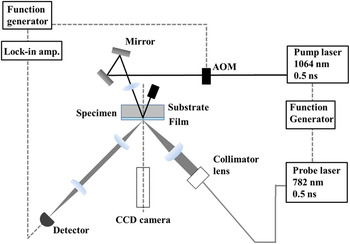
Figure 3 shows a schematic of our pulsed light heating thermoreflectance system for measuring the thermal diffusivity. Figure 4 shows typical thermoreflectance results for the trilayer Mo/(ATO or TTO)/Mo films, where the inner polycrystalline ATO or TTO layers were deposited at the O2 GFRs as shown in Figs. 1 and 2. We irradiated the bottom Mo layer (i.e., the Mo/substrate interface) with a 1064 nm pump laser to generate one-dimensional heat flow across the layered sample. Next, the temperature at the surface of the top Mo layer was detected by a 782 nm probe laser. The reflected probe beam was detected by a silicon photodiode. Because the thermoreflectance signal can be assumed to be proportional to temperature, Reference Taketoshi, Baba and Ono28 the signal rise time corresponds to the thermal diffusivity of the films. We analyzed the thermal diffusivities of the ATO and TTO films using a previously reported one-dimensional heat-flow model for trilayer films. Reference Baba14,Reference Yagi, Tamano, Sato, Taketoshi, Baba and Shigesato16,Reference Yagi, Oka, Okabe, Taketoshi, Baba and Shigesato22 The film thickness d Mo of the Mo layer was 100 nm, the thermal diffusivity κMo was 1.7 × 10⁻⁵ m2 s−1, and the heat capacity C Mo per unit volume was 2.53 × 10⁶ J m−3 K−1. Reference Barin and Platzki29 The ATO and TTO parameters were determined based on a heat capacity for SnO2 of 53.2 J mol−1 K−1 (Ref. Reference Oka, Kato, Yagi, Taketoshi, Baba and Shigesato23) and a density for SnO2 of 6950 kg m−3, Reference Oka, Kato, Yagi, Taketoshi, Baba, Ito and Shigesato24 which gives a heat capacity per unit volume of 2.45 × 10⁶ J m−3 K−1. We neglected the thermal boundary resistance between the outer Mo layer and the sandwiched inner layer because it should be considerably smaller than the total thermal resistance. Reference Yagi, Tamano, Sato, Taketoshi, Baba and Shigesato16,Reference Oka, Arisawa, Miyamura, Sato, Yagi, Taketoshi, Baba and Shigesato17,Reference Kawasaki, Yamashita, Oka, Yagi, Jia, Taketoshi, Baba and Shigesato21,Reference Oka, Kato, Yagi, Taketoshi, Baba and Shigesato23 Our measurements indicate that the thermal diffusivity of the polycrystalline ATO and TTO films is (1.8–2.0) × 10−6 and 1.9 × 10⁻⁶ m2 s−1, respectively. The different dopants (Sb and Ta) do not appear to significantly influence the thermal diffusivity.

FIG. 3. Schematic of the pulsed light heating thermoreflectance system.

FIG. 4. Temporal thermoreflectance of trilayer Mo/(ATO or TTO)/Mo films. Inner layer is (a) ATO and (b) TTO.
IV. DISCUSSION
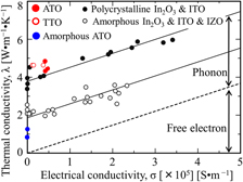
Figure 5 shows the thermal conductivity λ plotted as a function of electrical conductivity σ for polycrystalline ATO and TTO films and for the amorphous ATO film, where λ is derived from the measured thermal diffusivity and from the specific heat capacity Reference Grigoriev and Meilikhov30 and density Reference Samsonov.31 of SnO2. For comparison, λ is also plotted for polycrystalline ITO films and amorphous ITO and IZO films. Reference Ashida, Miyamura, Oka, Sato, Yagi, Taketoshi, Baba and Shigesato12 At equivalent σ, λ for polycrystalline ATO and TTO films is higher than that of the ITO and IZO films. The TCO films are highly degenerate: free electrons behave similar to those in a metal. Thus, both free electrons and phonons should contribute to heat transport. The thermal conductivity λ el carried by free electrons can be described by the Wiedemann–Franz law λ el = LTσ, where L is the Lorentz number (2.45 × 10⁻⁸ W Ω K−2) and T is absolute temperature. The dashed line in Fig. 5 gives the result for λ el calculated from the Wiedemann–Franz law. The thermal conductivity λ ph carried by phonons can be estimated by subtracting λ el from the measured total thermal conductivity: λ ph differs significantly between polycrystalline and amorphous films, possibly because phonon corresponds to an atomic vibrational motion and its propagation is affected by crystallization. For polycrystalline ATO and TTO films, λ ph is greater than that for polycrystalline ITO films. In general, λ ph for metal oxides increases with approaching unity for the atomic mass ratio of “metal and oxygen,” with a smaller unit cell, or with a simpler lattice structure (because of lattice vibrations or phonons). Reference Oka, Kimura, Yagi, Taketoshi, Baba and Shigesato18,Reference Tasaki, Oka, Yagi, Taketoshi, Baba, Kamiyama, Nakamura and Shigesato19,Reference Tsubota, Ohtaki, Eguchi and Arai32 Table I lists the metal/oxygen atomic mass ratio and the lattice structure for a base oxide material for various polycrystalline TCO films [i.e., ATO, TTO, ITO, Al-doped ZnO (AZO), and Nb-doped TiO2 (NTO)]. Table II summarizes the thermophysical and electrical properties of these TCOs and amorphous IZO. The atomic mass ratios of Sn/O and In/O are almost the same. SnO2 with a rutile structure has a considerably smaller unit cell and a simpler lattice structure than the bixbyite structure of In2O3, which may contribute significantly to higher λ ph for ATO and TTO films. The same scheme can be applied to λ ph of the other TCO materials, as shown in Table II.

FIG. 5. Thermal conductivity as a function of electrical conductivity for ATO film (solid red circles) and TTO film (open red circles). Dotted line shows thermal conductivity calculated by the Wiedemann–Franz law. For comparison, the thermal conductivity of a polycrystalline ITO film (solid black circles) and an amorphous ITO and IZO film (open black circles) Reference Ashida, Miyamura, Oka, Sato, Yagi, Taketoshi, Baba and Shigesato12 is also plotted.
TABLE I. Atomic mass ratio of metal and oxygen, and lattice structure for SnO2-, In2O3-, ZnO-, and TiO2-based TCO films.

TABLE II. Thermophysical and electrical properties of SnO2-, In2O3-, ZnO-, and TiO2-based TCO films.

In contrast, the dopant species (Sb or Ta) has a considerably smaller effect on λ ph than does the base-material species (SnO2 or In2O3). Although λ ph in ITO is almost constant irrespective of dopant concentration, Reference Ashida, Miyamura, Oka, Sato, Yagi, Taketoshi, Baba and Shigesato12 λ ph in NTO was reported to decrease with increasing dopant concentration. Reference Tasaki, Oka, Yagi, Taketoshi, Baba, Kamiyama, Nakamura and Shigesato19 The atomic weight ratio of Nb/Ti (1.94) is considerably greater than that of Sn/In (1.03), which should lead to more extensive phonon scattering in NTO than in ITO. Reference Tasaki, Oka, Yagi, Taketoshi, Baba, Kamiyama, Nakamura and Shigesato19 For ATO and TTO, the atomic mass ratios are Sb/Sn = 1.03 and Ta/Sn = 1.52, respectively. Currently, we cannot determine why λ ph is only slightly affected by dopant species (Sb or Ta). One hypothesis is that, for transparent conductive SnO2 films, the dopant concentration of Sb or Ta may be insufficient to significantly influence λ ph.
Finally, λ of undoped SnO2 single crystals was previously reported as 98 W m−1 K−1, Reference Turkes, Pluntke and Helbig36 approximately 20 times higher than ATO and TTO films. Lower λ of these films can be attributed to the polycrystalline structure, and to structural defects generated by the dopants or the high energy particles, such as O− bombarding on the growing film surface during sputter deposition. Reference Tsukamoto, Watanabe, Saito, Sato, Oka and Shigesato37–Reference Ito, Miyatake, Tsukamoto, Oka, Sato and Shigesato40
V. CONCLUSIONS
We measured the thermal diffusivity of 200-nm-thick ATO and TTO films by the pulsed light heating thermoreflectance method. ATO or TTO films sandwiched between 100-nm-thick Mo films [Mo/(ATO or TTO)/Mo] were fabricated by rf magnetron sputtering onto a fused silica substrate heated to 300 °C. During ATO and TTO film deposition, Ar–O2 or Ar–H2 gas mixtures were used to control the electrical conductivity of the films. The thermal diffusivities of the polycrystalline ATO and TTO films were measured to be (1.8–2.0) × 10−6 and 1.9 × 10⁻⁶ m2 s−1, respectively. The contribution of electrons to thermal transport is described by the Wiedemann–Franz law and that of phonons is almost constant, irrespective of the dopant species (Sb or Ta). Furthermore, the contribution of phonons to thermal transport is larger than that to polycrystalline ITO and amorphous ATO films. Compared with the effects of the base-material species and the structure (polycrystalline or amorphous), the dopant species has little effect on the thermophysical properties of transparent conductive ATO and TTO films. This knowledge allows us to form a strategy for choosing a material (base-material, dopant, structure) to optimize the thermal design for various industrial applications.
ACKNOWLEDGMENTS
This work was partially supported as a High-Tech Research Center project for private universities with matching funding from the Ministry of Education, Culture, Sports, Science and Technology (MEXT) of the Japanese Government.