


Crossref Citations
This article has been cited by the following publications. This list is generated based on data provided by Crossref.
Nguyen, Cong Thanh
Ohdaira, Keisuke
and
Matsumura, Hideki
2019.
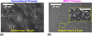
Control of Texture Size on As-Cut Crystalline Silicon by Microparticle-Assisted Texturing (MPAT) Process.
p.
0795.
Nguyen, Cong Thanh
Ohdaira, Keisuke
and
Matsumura, Hideki
2019.
Control of solution wettability on fine-textured crystalline silicon surface to obtain high-quality passivation for solar cells.
Applied Physics Letters,
Vol. 114,
Issue. 13,
Ko, Yohan
Park, HyunJung
Lee, Chanyong
Kang, Yoonmook
and
Jun, Yongseok
2020.
Recent Progress in Interconnection Layer for Hybrid Photovoltaic Tandems.
Advanced Materials,
Vol. 32,
Issue. 51,
Alasfour, Abdulwahab
Yu, Zhengshan J.
Weigand, William
Quispe, David
and
Holman, Zachary C.
2020.
Sub-micrometer random-pyramid texturing of silicon solar wafers with excellent surface passivation and low reflectance.
Solar Energy Materials and Solar Cells,
Vol. 218,
Issue. ,
p.
110761.
Chen, Bo
Yu, Zhengshan J.
Manzoor, Salman
Wang, Shen
Weigand, William
Yu, Zhenhua
Yang, Guang
Ni, Zhenyi
Dai, Xuezeng
Holman, Zachary C.
and
Huang, Jinsong
2020.
Blade-Coated Perovskites on Textured Silicon for 26%-Efficient Monolithic Perovskite/Silicon Tandem Solar Cells.
Joule,
Vol. 4,
Issue. 4,
p.
850.
Li, Yuqing
Sai, Hitoshi
Matsui, Takuya
Xu, Zhihao
Nguyen, Van Hoang
Kurokawa, Yasuyoshi
and
Usami, Noritaka
2022.
Nanopyramid Texture Formation by One‐Step Ag‐Assisted Solution Process for High‐Efficiency Monocrystalline Si Solar Cells.
Solar RRL,
Vol. 6,
Issue. 11,
Harter, Angelika
Mariotti, Silvia
Korte, Lars
Schlatmann, Rutger
Albrecht, Steve
and
Stannowski, Bernd
2023.
Double‐sided nano‐textured surfaces for industry compatible high‐performance silicon heterojunction and perovskite/silicon tandem solar cells.
Progress in Photovoltaics: Research and Applications,
Vol. 31,
Issue. 8,
p.
813.