


No CrossRef data available.
Article contents
Optimization of Cu(In,Ga)Se2 formation by regulating the stacked metal layers structure-the role of metallic growth
Published online by Cambridge University Press: 12 December 2016
Abstract
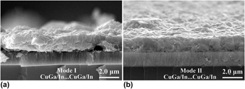
The absorber layers for chalcopyrite solar cells were fabricated by selenization of the stacked metal layers (SML). Co-sputtering and sequential sputtering methods were utilized to prepare the SML, and the variation of the stacking sequences and the effect of each stacked layer thickness were investigated. The stacking sequence of In/CuGa⋯In/CuGa was found having advantages in the SML growth and the average size of indium hillocks might be tailored by changing the thickness of each stacked layer. The SML in the stacking mode of In/CuGa⋯In/CuGa prepared while the thickness for each indium layer fixed at approximately 83 nm exhibited the desired morphology with evenly distributed indium hillocks in small diameters. The selenized ${\rm{CuI}}{{\rm{n}}_x}{\rm{G}}{{\rm{a}}_{1 - x}}{\rm{S}}{{\rm{e}}_2}$
(CIGS) layer showed a smooth surface and largest grain size with phase segregation being suppressed effectively. The hole mobility of the best CIGS layers reached 8.36 cm2/V s.
${\rm{CuI}}{{\rm{n}}_x}{\rm{G}}{{\rm{a}}_{1 - x}}{\rm{S}}{{\rm{e}}_2}$
(CIGS) layer showed a smooth surface and largest grain size with phase segregation being suppressed effectively. The hole mobility of the best CIGS layers reached 8.36 cm2/V s.
Keywords
- Type
- Articles
- Information
- Copyright
- Copyright © Materials Research Society 2016
References
REFERENCES
Jackson, P., Hariskos, D., Wuerz, R., Kiowski, O., Bauer, A., Friedlmeier, T.M., and Powalla, M.: Properties of Cu(In,Ga)Se2 solar cells with new record efficiencies up to 21.7%. Phys. Status Solidi RRL
9(1), 28–31 (2015).Google Scholar
Jager-Waldau, A.: Progress in chalcopyrite compound semiconductor research for photovoltaic applications and transfer of results into actual solar cell production. Sol. Energy Mater. Sol. Cells
95, 1509–1517 (2011).CrossRefGoogle Scholar
Koo, J., Jeon, S., Oh, M., Cho, H-I., Son, C., and Kim, W.K.: Optimization of Se layer thickness in Mo/CuGa/In/Se precursor for the formation of Cu(InGa)Se2 by rapid thermal annealing. Thin Solid Films
535, 148–153 (2013).Google Scholar
Frantz, J.A., Myers, J.D., Bekele, R.Y., Nguyen, V.Q., Sadowski, B.M., Maximenko, S.I., Walters, R.J., and Sanghera, J.S.: Recent Progress in Sputtered Cu(In,Ga)Se2 Absorbers for Photovoltaics (NOMA, NS3B.2, Boston, 2015); pp. 215.Google Scholar
Park, J. and Kim, W.K.: Effect of sputtering conditions of co-sputtered Cu–In–Ga precursors on Cu(InGa)Se2 photovoltaic absorber formation. Thin Solid Films
572, 61–67 (2014).Google Scholar
Li, Z-H., Cho, E-S., and Kwon, S.J.: Selenization annealing effect of DC-sputtered metallic precursors using the rapid thermal process for Cu(In,Ga)Se2 thin film solar cells. Thin Solid Films
547, 156–162 (2013).CrossRefGoogle Scholar
Han, J-F., Liao, C., Jiang, T., Xie, H-M., Zhao, K., and Besland, M-P.: An optimized In–CuGa metallic precursors for chalcopyrite thin films. Thin Solid Films
545, 251–256 (2013).Google Scholar
Chung, C.H., Kim, S.D., Kim, H.J., Adurodija, F.O., Yoon, K.H., and Song, J.: Phase formation and control of morphology in sputtered Cu–In alloy layers. Solid State Commun.
126, 185–190 (2003).CrossRefGoogle Scholar
Başol, B.M., Kapur, V.K., Halani, A., Leidholm, C.R., Sharp, J., Sites, J.R., Swartzlander, A., Matson, R., and Ullal, H.: Cu (In,Ga)Se2 thin films and solar cells prepared by selenization of metallic precursors. J. Vac. Sci. Technol. A
14(4), 2251–2256 (1996).CrossRefGoogle Scholar
Park, H., Kim, S.C., Lee, S-H., Koo, J., Lee, S.H., Jeon, C-W., Yoon, S., and Kim, W.K.: Effect of precursor structure on Cu(InGa)Se2 formation by reactive annealing. Thin Solid Films
519, 7245–7249 (2011).CrossRefGoogle Scholar
Wider, H., Gimple, V., Evenson, W., Schatz, G., Jaworski, J., Prokop, J., and Marszalek, M.: Surface alloying of indium on Cu(111). J. Phys.: Condens. Matter
15, 1909–1919 (2003).Google Scholar
Wei, H.L., Zhang, L., Liu, Z., Huang, H., and Zhang, X.: Spontaneous growth of indium nanostructures. J. Cryst. Growth
297, 300–305 (2006).Google Scholar
Wei, H-L., Zhang, X-X., and Huang, H-C.: Spontaneous hillock growth on indium film surface. Chin. Phys. Lett.
23(7), 1880 (2006).Google Scholar
Theron, C.C., Ndwandwe, O.M., Lombaard, J.C., and Pretorius, R.: First phase formation at interfaces: Comparison between Walser-Bené and effective heat of formation model. Mater. Chem. Phys.
46(2–3), 238–247 (1996).Google Scholar
Baji, Z., Lábadi, Z., Molnár, G., Pécz, B., Tóth, A.L., Tóth, J., Csik, A., and Bársony, I.: Post-selenization of stacked precursor layers for CIGS. Vacuum
92, 44–51 (2013).Google Scholar
Han, J-F., Liao, C., Gautron, E., Jiang, T., Xie, H-M., Zhao, K., and Besland, M-P.: A study of different selenium sources in the synthesis processes of chalcopyrite semiconductors. Vacuum
105, 46–51 (2014).Google Scholar
Mainz, R., Weber, A., Rodriguez-Alvarez, H., Levcenko, S., Klaus, M., Pistor, P., Klenk, R., and Schock, H-W.: Time-resolved investigation of Cu(In,Ga)Se2 growth and Ga gradient formation during fast selenisation of metallic precursors. Prog. Photovolt: Res. Appl.
23(9), 1131–1143 (2015).CrossRefGoogle Scholar
Hanket, G.M., Shafarman, W.N., McCandless, B.E., and Birkmire, R.W.: Incongruent reaction of Cu-(InGa) intermetallic precursors in H2Se and H2S. J. Appl. Phys.
102, 074922 (2007).CrossRefGoogle Scholar
Klenk, R., Walter, T., Schock, H-W., and Cahen, D.: A model for the successful growth of polycrystalline films of CuInSe2 by multisource physical vacuum evaporation. Adv. Mater.
5(2), 114–119 (1993).CrossRefGoogle Scholar
Liu, J., Xiang Wei, A., Zhao, Y., and Yan, Z.Q.: Effect of stacking type in precursors on composition, morphology and electrical properties of the CIGS films. J. Mater Sci: Mater Electron
24, 2553–2557 (2013).Google Scholar