


No CrossRef data available.
Article contents
Low-temperature fabrication of nanocrystalline silicon thin films on mechanically flexible substrates by vacuum arc discharge
Published online by Cambridge University Press: 19 April 2011
Abstract
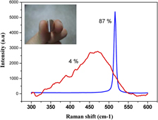
Nanocrystalline silicon thin films were fabricated using a vacuum arc discharge technique. These thin films can be deposited on plastic substrates effectively when cooled by a cryogenic substrate holder. We used single crystal silicon wafers as both the electrodes to ignite the vacuum arc and the silicon ion source to deposit thin films. This resulted in nanocrystalline silicon clusters embedded in the amorphous silicon matrix. This thin film has highly crystalline volume (≈87%), which enhanced the absorption in wide range of wavelengths. Without ion implantation, the in situ doping of p- or n-type thin films can also be achieved. This thin film deposition process has its potential for fabricating thin film transistors and photovoltaic cells on plastic substrates at fairly low production costs.
Keywords
- Type
- Articles
- Information
- Copyright
- Copyright © Materials Research Society 2011
References
REFERENCES
2.Chan, K.-Y., Kirchhoff, J., Gordijn, A., Knipp, D., and Stiebig, H.: Ambipolar microcrystalline silicon thin-film transistors. Thin Solid Films 517, 6383 (2009).CrossRefGoogle Scholar
3.Lin, J.-L., Sah, W.-J., and Lee, S.-C.: Amorphous-silicon thin-film transistors with very high field-effect mobility. IEEE Electron Device Lett. 12, 120 (1991).Google Scholar
4.Cabarrocas, P., Morral, A., Lebib, S., and Poissant, Y.: Plasma production of nanocrystalline silicon particles and polymorphous silicon thin films for large-area electronic devices. Pure Appl. Chem. 74, 359 (2002).CrossRefGoogle Scholar
5.Meier, J., FluÈckiger, R., Keppner, H., and Shah, A.: Complete microcrystalline p‐i‐n solar cell. Appl. Phys. Lett. 65, 860 (1994).CrossRefGoogle Scholar
6.Xu, Y., Liao, X., Kong, G., Zeng, X., Hu, Z., Diao, H., and Zhang, S.: Microstructure characterization of transition films from amorphous to nanocrocrystalline silicon. J. Cryst. Growth 256, 27 (2003).CrossRefGoogle Scholar
7.Klein, S., Finger, F., Carius, R., Wagner, H., and Stutzmann, M.: Intrinsic amorphous and microcrystalline silicon by hot-wire-deposition for thin film solar cell applications. Thin Solid Films 395, 305 (2001).CrossRefGoogle Scholar
8.Armin, G.A.: Fabrication and characterisation of crystalline silicon thin-film materials for solar cells. Thin Solid Films 511, 26 (2006).Google Scholar
9.Valipa, M.S., Sriraman, S., Aydil, E.S., and Maroudas, D.: Hydrogen-induced crystallization of amorphous Si thin films. II. Mechanisms and energetics of hydrogen insertion into Si–Si bonds. J. Appl. Phys. 100, 053515 (2006).CrossRefGoogle Scholar
10.Chua, D.H.C., Teo, K.B.K., Tsai, T.H., Milne, W.I., Sheeja, D., Tay, B.K., and Schneider, D.: Correlation of surface, mechanical and microproperties of tetrahedral amorphous carbon films deposited under different magnetic confinement condition. Appl. Surf. Sci. 221, 455 (2004).CrossRefGoogle Scholar
11.Suzuki, Y., Niino, F., and Katoh, K.: Low-resistivity ITO films by dc arc discharge ion plating for high duty LCDs. J. Non-Cryst. Solids 218, 30 (1997).CrossRefGoogle Scholar
12.Bustarret, E., Hachicha, M.A., and Brunel, M.: Experimental determination of the nanocrystalline volume fraction in silicon thin films from Raman spectroscopy. Appl. Phys. Lett. 52, 1675 (1988).CrossRefGoogle Scholar
13.Anders, A.: Ion charge state distributions of vacuum arc plasmas: The origin of species. Phys. Rev. E: Stat. Phys. Plasmas Fluids Relat. Interdisciplin. Top. 55(1), 969 (1997).CrossRefGoogle Scholar
14.Cuomo, J.J., Pappas, D.L., Bruley, J., Doyle, J.P., and Saenger, K.L.: Vapor deposition processes for amorphous carbon films with sp3 fractions approaching diamond. J. Appl. Phys. 70(3), 1706 (1991).CrossRefGoogle Scholar
15.Cabarrocas, P.R.I., Morral, A.F.I., Lebib, S., and Poissant, Y.: Plasma production of nanocrystalline silicon particles and polymorphous silicon thin films for large-area electronic devices. Pure Appl. Chem. 74(3), 369 (2002).CrossRefGoogle Scholar
16.Fallon, P.J., Veerasamy, V.S., Davis, C.A., Robertson, J., Amaratunga, G.A.J., Milne, W.I., and Koskinen, J.: Properties of filtered ion beam deposited diamondlike carbon as a function of ion energy. Phys. Rev. B 48, 4777 (1993).CrossRefGoogle ScholarPubMed
17.Robertson, J.: The deposition mechanism of diamond-like a-C and a-C: H. Diamond Related Materials 3, 361 (1994).CrossRefGoogle Scholar
18.Lifshitz, Y., Kasi, S.R., Rabalais, J.W., and Eckstein, W.: Suplantation model for film growth from hyperthermal species. Phys. Rev. B 41, 10468 (1990).CrossRefGoogle ScholarPubMed
19.Bilek, M.M.M., Chhowalla, M., Weiler, M., and Milne, W.I.: Ion energy and plasma characterization in a silicon filtered cathodic vacuum arc. J. Appl. Phys. 79(3), 1287 (1996).CrossRefGoogle Scholar
20.Kimura, Y. and Katoda, T.: Effects of strain on crystallization of amorphous silicon characterized by laser Raman spectroscopy. Appl. Surf. Sci. 117, 790 (1997).CrossRefGoogle Scholar
21.Paillard, V., Puech, P., Laguna, M.A., Carles, R., Kohn, B., and Huisken, F.: Improved one-phonon confinement model for an accurate size determination of silicon nanocrystals. J. Appl. Phys. 86, 1921 (1999).CrossRefGoogle Scholar
22.Schroder, D.K.: Semiconductor Material and Device Characterization, 3rd ed. (Wiley-Interscience, Hoboken, NJ, 2006) p. 14.Google Scholar
23.Sze, S.: Physics of Semiconductor Devices, 3rd ed. (Wiley, New York, NY, 2007) p. 32.Google Scholar