Hostname: page-component-8448b6f56d-jr42d Total loading time: 0 Render date: 2024-04-19T15:20:38.373Z Has data issue: false hasContentIssue false

Effect of Gd3+ doping on structural, morphological, optical, dielectric, and nonlinear optical properties of high-quality PbI2 thin films for optoelectronic applications

Published online by Cambridge University Press:  28 June 2019

Mohd. Shkir*
Affiliation:
Advanced Functional Materials & Optoelectronics Laboratory (AFMOL), Department of Physics, College of Science, King Khalid University, Abha 61413, Saudi Arabia
Salem AlFaify*
Affiliation:
Advanced Functional Materials & Optoelectronics Laboratory (AFMOL), Department of Physics, College of Science, King Khalid University, Abha 61413, Saudi Arabia
*
a)Address all correspondence to this author. e-mail: saalfaify@kku.edu.sa
Get access

Abstract

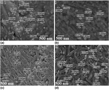
Herein, we present the fabrication and characterization of Gd:PbI2 thin films from low-cost material using a cost-effective spin-coating technique by taking the Gd content as 1.0, 2.0, and 3.0 wt% in PbI2. Single-phase and good crystallinity films oriented along the c-axis were confirmed by X-ray diffraction and FT-Raman spectroscopy. Size of crystallites increased with Gd concentration and was estimated to be in the range of 16–32 nm. Determination of morphology and size of grains (50–103 nm), and elemental confirmation were carried out by SEM/EDX analysis. Optical transparency of fabricated films was found to be in the range of 72–92%. The energy gap is reduced from 2.31 to 2.05 eV; this makes Gd:PbI2 films highly applicable in solar cells. The stable value of refractive index is estimated to be in the range of 1.85–2.3. Dielectric constant was observed to be reduced with doping and in the range of 2.5–35, and ac conductivity was also reduced by doping; however, both were enhanced with frequency. The values of χ(1), χ(3), and n(2) are found to be in the range of 0.15 to 2.5, 8 × 10⁻¹⁴ to 6.5 × 10⁻⁹, and 5 × 10⁻¹² to 4 × 10⁻⁸, respectively.

Type
Article
Copyright
Copyright © Materials Research Society 2019 

Access options

Get access to the full version of this content by using one of the access options below. (Log in options will check for institutional or personal access. Content may require purchase if you do not have access.)

References

Saliba, M., Matsui, T., Seo, J-Y., Domanski, K., Correa-Baena, J-P., Nazeeruddin, M.K., Zakeeruddin, S.M., Tress, W., Abate, A., and Hagfeldt, A.: Cesium-containing triple cation perovskite solar cells: Improved stability, reproducibility and high efficiency. Energy Environ. Sci. 9, 1989 (2016).CrossRefGoogle ScholarPubMed
Park, B-w., Kedem, N., Kulbak, M., Yang, W.S., Jeon, N.J., Seo, J., Kim, G., Kim, K.J., Shin, T.J., and Hodes, G.: Understanding how excess lead iodide precursor improves halide perovskite solar cell performance. Nat. Commun. 9, 3301 (2018).CrossRefGoogle ScholarPubMed
Zhang, J., Huang, Y., Tan, Z., Li, T., Zhang, Y., Jia, K., Lin, L., Sun, L., Chen, X., and Li, Z.: Low-temperature heteroepitaxy of 2D PbI2/graphene for large-area flexible photodetectors. Adv. Mater. 30, 1803194 (2018).CrossRefGoogle Scholar
Melvin, A.A., Stoichkov, V.D., Kettle, J., Mogilyansky, D., Katz, E.A., and Visoly-Fisher, I.: Lead iodide as a buffer layer in UV-induced degradation of CH3NH3PbI3 films. Sol. Energy 159, 794 (2018).CrossRefGoogle Scholar
Chen, H-B., Ding, X-H., Pan, X., Hayat, T., Alsaedi, A., Ding, Y., and Dai, S-Y.: Incorporating C60 as nucleation sites optimizing PbI2 films to achieve perovskite solar cells showing excellent efficiency and stability via vapor-assisted deposition method. ACS Appl. Mater. Interfaces 10, 2603 (2018).CrossRefGoogle ScholarPubMed
Sun, K., Hu, Z., Shen, B., Lu, C., Huang, L., Zhang, J., Zhang, J., and Zhu, Y.: Lewis acid–base interaction-induced porous PbI2 film for efficient planar perovskite solar cells. ACS Appl. Energy Mater. 1, 2114 (2018).CrossRefGoogle Scholar
Shkir, M., AlFaify, S., Yahia, I.S., Hamdy, M.S., Ganesh, V., and Algarni, H.: Facile hydrothermal synthesis and characterization of cesium-doped PbI2 nanostructures for optoelectronic, radiation detection and photocatalytic applications. J. Nanopart. Res. 19, 328 (2017).CrossRefGoogle Scholar
Abbaszadeh, S. and Levin, C.S.: Direct conversion semiconductor detectors for radiation imaging. In Semiconductor Radiation Detectors Technology and Applications, Vol. 1 (Salim Reza, CRC Press, Florida, 2017); p. 21.Google Scholar
Liu, X., Ha, S.T., Zhang, Q., de la Mata, M., Magen, C., Arbiol, J., Sum, T.C., and Xiong, Q.: Whispering gallery mode lasing from hexagonal shaped layered lead iodide crystals. ACS Nano 9, 687 (2015).CrossRefGoogle ScholarPubMed
Condeles, J.F. and Mulato, M.: Crystalline texture and mammography energy range detection studies of pyrolysed lead iodide films: Effects of solution concentration. Mater. Chem. Phys. 166, 190 (2015).CrossRefGoogle Scholar
Condeles, J., Lofrano, R., Rosolen, J., and Mulato, M.: Stoichiometry, surface and structural characterization of lead iodide thin films. Braz. J. Phys. 36, 320 (2006).CrossRefGoogle Scholar
Condeles, J. and Mulato, M.: Polycrystalline lead iodide films produced by solution evaporation and tested in the mammography X-ray energy range. J. Phys. Chem. Solids 89, 39 (2016).CrossRefGoogle Scholar
Li, W., Yang, J., Jiang, Q., Li, R., and Zhao, L.: Electrochemical deposition of PbI2 for perovskite solar cells. Sol. Energy 159, 300 (2018).CrossRefGoogle Scholar
Fan, H., Ren, X., Yang, Z., Ren, X., Xiao, F., Zi, W., Yin, M., and Liu, S.F.: Thickness influence on optical and electrical properties of PbI2 films prepared by pulsed laser deposition. Sci. Adv. Mater. 10, 701 (2018).CrossRefGoogle Scholar
Al-Daraghmeh, T.M., Saleh, M.H., Ahmad, M.J.A., Bulos, B.N., Shehadeh, K.M., and Jafar, M.M.A-G.: Electrical transport mechanisms and photoconduction in undoped crystalline flash-evaporated lead iodide thin films. J. Electron. Mater. 47, 1806 (2018).CrossRefGoogle Scholar
Wang, Y., Gan, L., Chen, J., Yang, R., and Zhai, T.: Achieving highly uniform two-dimensional PbI2 flakes for photodetectors via space confined physical vapor deposition. Sci. Bull. 62, 1654 (2017).CrossRefGoogle Scholar
Wang, Y., Sun, Y-Y., Zhang, S., Lu, T-M., and Shi, J.: Band gap engineering of a soft inorganic compound PbI2 by incommensurate van der Waals epitaxy. Appl. Phys. Lett. 108, 013105 (2016).CrossRefGoogle Scholar
Zhu, X., Sun, H., Yang, D., and Zheng, X.: Growth, surface treatment and characterization of polycrystalline lead iodide thick films prepared using close space deposition technique. Nucl. Instrum. Methods Phys. Res., Sect. A 691, 10 (2012).CrossRefGoogle Scholar
Ghosh, T., Bandyopadhyay, S., Roy, K., Kar, S., Lahiri, A., Maiti, A., and Goswami, K.: Optical and structural properties of lead iodide thin films prepared by vacuum evaporation method. Cryst. Res. Technol. 43, 959 (2008).CrossRefGoogle Scholar
Shkir, M., Abbas, H., and Khan, Z.R.: Effect of thickness on the structural, optical and electrical properties of thermally evaporated PbI2 thin films. J. Phys. Chem. Solids 73, 1309 (2012).CrossRefGoogle Scholar
Shah, K.S., Bennett, P.R., Klugerman, M.B., Moy, L.P., Entine, G., Ouimette, D.R., and Aikens, R.S.: Lead iodide films for X-ray imaging. Intern. Soc. Opt. Phot. 3032, 395 (1997).Google Scholar
Xiao, M., Huang, F., Huang, W., Dkhissi, Y., Zhu, Y., Etheridge, J., Gray-Weale, A., Bach, U., Cheng, Y.B., and Spiccia, L.: A fast deposition-crystallization procedure for highly efficient lead iodide perovskite thin-film solar cells. Angew. Chem., Int. Ed. 53, 9898 (2014).CrossRefGoogle ScholarPubMed
Wang, W-T., Sharma, J., Chen, J-W., Kao, C-H., Chen, S-Y., Chen, C-H., Feng, Y-C., and Tai, Y.: Nanoparticle-induced fast nucleation of pinhole-free PbI2 film for ambient-processed highly-efficient perovskite solar cell. Nano Energy 49, 109 (2018).CrossRefGoogle Scholar
Kuiry, S., Roy, S., and Bose, S.: Estimation of hole conductivity in Ag-doped lead iodide film. Mater. Res. Bull. 33, 611 (1998).CrossRefGoogle Scholar
Bhavsar, D. and Saraf, K.: Optical and structural properties of Zn-doped lead iodide thin films. Mater. Chem. Phys. 78, 630 (2003).CrossRefGoogle Scholar
Bhavsar, D.: Transmittance and reflectance properties of Cu-doped and undoped lead iodide thin films deposited by vacuum evaporation technique. Arch. Appl. Sci. Res. 4, 1106 (2012).Google Scholar
Dmitriev, Y., Bennett, P.R., Cirignano, L.J., Klugerman, M., and Shah, K.S.: PbI2 thick films: Growth, properties, and problems. Nucl. Instrum. Methods Phys. Res., Sect. A 584, 165 (2008).CrossRefGoogle Scholar
Shkir, M., Yahia, I.S., Ganesh, V., Algarni, H., and AlFaify, S.: Facile hydrothermal-assisted synthesis of Gd3+ doped PbI2 nanostructures and their characterization. Mater. Lett. 176, 135 (2016).CrossRefGoogle Scholar
Shkir, M. and AlFaify, S.: Tailoring the structural, morphological, optical and dielectric properties of lead iodide through Nd3+ doping. Sci. Rep. 7, 16091 (2017).CrossRefGoogle ScholarPubMed
AlFaify, S., Shkir, M., and Ganesh, V.: Facile one pot synthesis of novel Hg2+ doped PbI2 nanostructures for optoelectronic and radiation shielding applications. Mater. Sci. Semicond. Process. 83, 231 (2018).CrossRefGoogle Scholar
Shkir, M., Ganesh, V., Yahia, I., and AlFaify, S.: Microwave-synthesis of La3+ doped PbI2 nanosheets (NSs) and their characterizations for optoelectronic applications. J. Mater. Sci.: Mater. Electron. 29, 15838 (2018).Google Scholar
Yahia, I. and Abutalib, M.: Synthesis, Raman spectroscopy and dielectric properties of Ag:Mn co-doped nanostructured PbI2 for solid state radiation detectors. J. Mol. Struct. 1138, 215 (2017).Google Scholar
Yahia, I., Shkir, M., Ganesh, V., Abutalib, M., Zahran, H., and Alfaify, S.: Facile microwave-assisted synthesis of Al:Mn co-doped PbI2 nanosheets: Structural, vibrational, morphological, dielectric and radiation activity studies. Mater. Sci.-Pol. 36, 320 (2018).CrossRefGoogle Scholar
Shkir, M., Yahia, I.S., Ganesh, V., Bitla, Y., Ashraf, I.M., Kaushik, A., and AlFaify, S.: A facile synthesis of Au-nanoparticles decorated PbI2 single crystalline nanosheets for optoelectronic device applications. Sci. Rep. 8, 13806 (2018).CrossRefGoogle ScholarPubMed
Ismail, R.A., Mousa, A., and Amin, M.H.: Synthesis of hybrid Au@PbI2 core–shell nanoparticles by pulsed laser ablation in ethanol. Mater. Res. Express 5, 115024 (2018).CrossRefGoogle Scholar
Shkir, M., Taukeer Khan, M., Ganesh, V., Yahia, I.S., Ul Haq, B., Almohammedi, A., Patil, P.S., Maidur, S.R., and AlFaify, S.: Influence of Dy doping on key linear, nonlinear and optical limiting characteristics of SnO2 films for optoelectronic and laser applications. Opt. Laser Technol. 108, 609 (2018).CrossRefGoogle Scholar
Shkir, M., Khan, M.T., Khan, A., El-Toni, A.M., Aldalbahi, A., and AlFaify, S.: Facilely synthesized Cu:PbS nanoparticles and their structural, morphological, optical, dielectric and electrical studies for optoelectronic applications. Mater. Sci. Semicond. Process. 96, 16 (2019).CrossRefGoogle Scholar
El-Kadry, N., Ashour, A., and Mahmoud, S.: Structural dependence of dc electrical properties of physically deposited CdTe thin films. Thin Solid Films 269, 112 (1995).CrossRefGoogle Scholar
Kasi, G.K., Dollahon, N.R., and Ahmadi, T.S.: Fabrication and characterization of solid PbI2 nanocrystals. J. Phys. D: Appl. Phys. 40, 1778 (2007).CrossRefGoogle Scholar
Wangyang, P., Sun, H., Zhu, X., Yang, D., and Gao, X.: Mechanical exfoliation and Raman spectra of ultrathin PbI2 single crystal. Mater. Lett. 168, 68 (2016).CrossRefGoogle Scholar
Sears, W.M., Klein, M., and Morrison, J.: Polytypism and the vibrational properties of PbI2. Phys. Rev. B 19, 2305 (1979).CrossRefGoogle Scholar
Shakir, M., Kushwaha, S., Maurya, K., Bhagavannarayana, G., and Wahab, M.: Characterization of ZnSe nanoparticles synthesized by microwave heating process. Solid State Commun. 149, 2047 (2009).CrossRefGoogle Scholar
Shkir, M., Aarya, S., Singh, R., Arora, M., Bhagavannarayana, G., and Senguttuvan, T.: Synthesis of ZnTe nanoparticles by microwave irradiation technique, and their characterization. Nanosci. Nanotechnol. Lett. 4, 405 (2012).CrossRefGoogle Scholar
Mohd, S., Ashraf, I.M., and AlFaify, S.: Surface area, optical and electrical studies on PbS nanosheets for visible light photo-detector application. Phys. Scr. 94, 025801 (2019).Google Scholar
AlFaify, S. and Shkir, M.: A facile one pot synthesis of novel pure and Cd doped PbI2 nanostructures for electro-optic and radiation detection applications. Opt. Mater. 88, 417 (2019).CrossRefGoogle Scholar
Alfaify, S. and Shkir, M.: A one pot room temperature synthesis of pure and Zn doped PbI2 nanostructures and their structural, morphological, optical, dielectric and radiation studies. J. Nanoelectron. Optoelectron. 14, 255 (2019).CrossRefGoogle Scholar
Shkir, M., AlFaify, S., Yahia, I.S., Ganesh, V., and Shoukry, H.: Microwave-assisted synthesis of Gd3+ doped PbI2 hierarchical nanostructures for optoelectronic and radiation detection applications. Phys. B 508, 41 (2017).CrossRefGoogle Scholar
Zhu, X., Wei, Z., Jin, Y., and Xiang, A.: Growth and characterization of a PbI2 single crystal used for gamma ray detectors. Cryst. Res. Technol. 42, 456 (2007).CrossRefGoogle Scholar
Shkir, M., Khan, A., El-Toni, A.M., Aldalbahi, A., Yahia, I.S., and AlFaify, S.: Structural, morphological, opto-nonlinear-limiting studies on Dy:PbI2/FTO thin films derived facilely by spin coating technique for optoelectronic technology. J. Phys. Chem. Solids 130, 189 (2019).CrossRefGoogle Scholar
Khan, M.T., Shkir, M., Almohammedi, A., and AlFaify, S.: Fabrication and characterization of La doped PbI2 nanostructured thin films for opto-electronic applications. Solid State Sci. 90, 95 (2019).CrossRefGoogle Scholar
Ilanchezhiyan, P., Mohan Kumar, G., Vinu, A., Al-Deyab, S.S., and Jayavel, R.: Structural and optical properties of Dy doped ZnO thin films prepared by pyrolysis technique. Internet J. Nanotechnol. 7, 1087 (2010).CrossRefGoogle Scholar
Arif, M., Shkir, M., AlFaify, S., Sanger, A., Vilarinho, P.M., and Singh, A.: Linear and nonlinear optical investigations of N:ZnO/ITO thin films system for opto-electronic functions. Opt. Laser Technol. 112, 539 (2019).CrossRefGoogle Scholar
Shkir, M., Ganesh, V., AlFaify, S., and Yahia, I.S.: Structural, linear and third order nonlinear optical properties of drop casting deposited high quality nanocrystalline phenol red thin films. J. Mater. Sci.: Mater. Electron. 28, 10573 (2017).Google Scholar
Buckman, A., Hong, N., and Wilson, D.: Large refractive-index change in PbI 2 films by photolysis at 150–180 °C. J. Opt. Soc. Am. 65, 914 (1975).CrossRefGoogle Scholar
Panda, D. and Tseng, T-Y.: Growth, dielectric properties, and memory device applications of ZrO2 thin films. Thin Solid Films 531, 1 (2013).CrossRefGoogle Scholar
Ren, W., Trolier-McKinstry, S., Randall, C.A., and Shrout, T.R.: Bismuth zinc niobate pyrochlore dielectric thin films for capacitive applications. J. Appl. Phys. 89, 767 (2000).CrossRefGoogle Scholar
Moazzami, R., Hu, C., and Shepherd, W.H.: Electrical characteristics of ferroelectric PZT thin films for DRAM applications. IEEE Trans. Electron Devices 39, 2044 (1992).CrossRefGoogle Scholar
Chaneliere, C., Autran, J.L., Devine, R.A.B., and Balland, B.: Tantalum pentoxide (Ta2O5) thin films for advanced dielectric applications. Mater. Sci. Eng., R 22, 269 (1998).CrossRefGoogle Scholar
Mohd, S., Khan, Z.R., Hamdy, M.S., Algarni, H., and AlFaify, S.: A facile microwave-assisted synthesis of PbMoO4 nanoparticles and their key characteristics analysis: A good contender for photocatalytic applications. Mater. Res. Express 5, 095032 (2018).Google Scholar
Usha, K., Sivakumar, R., and Sanjeeviraja, C.: Optical constants and dispersion energy parameters of NiO thin films prepared by radio frequency magnetron sputtering technique. J. Appl. Phys. 114, 123501 (2013).CrossRefGoogle Scholar
Kim, M-S., Yim, K-G., Son, J-S., and Leem, J-Y.: Effects of Al concentration on structural and optical properties of Al-doped ZnO thin films. Bull. Korean Chem. Soc. 33, 1235 (2012).CrossRefGoogle Scholar
Strogatz, S.H.: Nonlinear Dynamics and Chaos: With Applications to Physics, Biology, Chemistry, and Engineering (CRC Press, Boca Raton, Florida, 2018).CrossRefGoogle Scholar
Sutter, E.E.: A deterministic approach to nonlinear systems analysis. In Nonlinear Vision: Determination of Neural Receptive Fields, Function, and Networks, E.E. Sutter, ed. (CRC Press, Boca Raton, Florida, 2018); p. 171.CrossRefGoogle Scholar
Luo, M., Liang, F., Song, Y., Zhao, D., Xu, F., Ye, N., and Lin, Z.: M2B10O14F6 (M = Ca, Sr): Two noncentrosymmetric alkaline earth fluorooxoborates as promising next-generation deep-ultraviolet nonlinear optical materials. J. Am. Chem. Soc. 140, 3884 (2018).CrossRefGoogle ScholarPubMed
Peng, G., Tang, Y-H., Lin, C., Zhao, D., Luo, M., Yan, T., Chen, Y., and Ye, N.: Exploration of new UV nonlinear optical materials in the sodium–zinc fluoride carbonates system with the discovery of a new regulation mechanism for the arrangement of [CO3]2− groups. J. Mater. Chem. C 6, 6526 (2018).CrossRefGoogle Scholar
Zhang, B., Han, G., Wang, Y., Chen, X., Yang, Z., and Pan, S.: Expanding frontiers of ultraviolet nonlinear optical materials with fluorophosphates. Chem. Mater. 30, 5397 (2018).CrossRefGoogle Scholar
Karuppanan, N. and Kalainathan, S.: A new nonlinear optical stilbazolium family crystal of (E)-1-Ethyl-2-(4-nitrostyryl)pyridin-1-ium iodide: Synthesis, crystal structure, and its third-order nonlinear optical properties. J. Phys. Chem. C 122, 4572 (2018).CrossRefGoogle Scholar
Alam, M.Z., Schulz, S.A., Upham, J., De Leon, I., and Boyd, R.W.: Large optical nonlinearity of nanoantennas coupled to an epsilon-near-zero material. Nat. Photon. 12, 79 (2018).CrossRefGoogle Scholar
Sandeep, K., Bhat, S., and Dharmaprakash, S.: Nonlinear absorption properties of ZnO and Al doped ZnO thin films under continuous and pulsed modes of operations. Opt. Laser Technol. 102, 147 (2018).CrossRefGoogle Scholar
Bannur, M., Antony, A., Maddani, K., Poornesh, P., Rao, A., and Choudhari, K.: Tailoring the nonlinear optical susceptibility χ(3), photoluminescence and optical band gap of nanostructured SnO2 thin films by Zn doping for photonic device applications. Phys. E 103, 348 (2018).CrossRefGoogle Scholar
Shkir, M., Ganesh, V., AlFaify, S., Yahia, I., and Zahran, H.: Tailoring the linear and nonlinear optical properties of NiO thin films through Cr3+ doping. J. Mater. Sci.: Mater. Electron. 29, 6446 (2018).Google Scholar
Talwatkar, S., Sunatkari, A., Tamgadge, Y., and Muley, G.: Nonlinear optical properties of Nd3+–Li+ co-doped ZnS-PVP thin films. In AIP Conference Proceedings, Vol. 1942 (AIP Publishing, College Park, Maryland, 2018); p. 080060.Google Scholar
Shkir, M., Arif, M., Ganesh, V., Manthrammel, M.A., Singh, A., Maidur, S.R., Patil, P.S., Yahia, I.S., Algarni, H., and AlFaify, S.: Linear, third order nonlinear and optical limiting studies on MZO/FTO thin film system fabricated by spin coating technique for electro-optic applications. J. Mater. Res. 33, 3880 (2018).CrossRefGoogle Scholar
Frumar, M., Jedelský, J., Frumarova, B., Wagner, T., and Hrdlička, M.: Optically and thermally induced changes of structure, linear and non-linear optical properties of chalcogenides thin films. J. Non-Cryst. Solids 326, 399 (2003).CrossRefGoogle Scholar
Adair, R., Chase, L., and Payne, S.A.: Nonlinear refractive index of optical crystals. Phys. Rev. B 39, 3337 (1989).CrossRefGoogle ScholarPubMed
Ticha, H. and Tichy, L.: Semiempirical relation between non-linear susceptibility (refractive index), linear refractive index and optical gap and its application to amorphous chalcogenides. J. Optoelectron. Adv. Mater. 4, 381 (2002).Google Scholar
Fournier, J. and Snitzer, E.: The nonlinear refractive index of glass. IEEE J. Quantum Electron. 10, 473 (1974).CrossRefGoogle Scholar
Wang, C.C.: Empirical relation between the linear and the third-order nonlinear optical susceptibilities. Phys. Rev. B 2, 2045 (1970).CrossRefGoogle Scholar
Wynne, J.: Nonlinear optical spectroscopy of χ(3) in LiNbO3. Phys. Rev. Lett. 29, 650 (1972).CrossRefGoogle Scholar
Nasu, H. and Mackenzie, J.D.: Nonlinear optical properties of glasses and glass or gel-based composites. Opt. Eng. 26, 262102 (1987).CrossRefGoogle Scholar
Sharma, P. and Katyal, S.: Linear and nonlinear refractive index of As–Se–Ge and Bi doped As–Se–Ge thin films. J. Appl. Phys. 107, 113527 (2010).CrossRefGoogle Scholar
Ganesh, V., Yahia, I., AlFaify, S., and Shkir, M.: Sn-doped ZnO nanocrystalline thin films with enhanced linear and nonlinear optical properties for optoelectronic applications. J. Phys. Chem. Solids 100, 115 (2017).CrossRefGoogle Scholar
Shaaban, E., El-Hagary, M., Hassan, H.S., Ismail, Y.A., Emam-Ismail, M., and Ali, A.: Structural, linear and nonlinear optical properties of co-doped ZnO thin films. Appl. Phys. A 122, 20 (2016).CrossRefGoogle Scholar
Supplementary material: PDF

Shkir and AlFaify supplementary material

Figure S1

Download Shkir and AlFaify supplementary material(PDF)
PDF 245.8 KB