Hostname: page-component-77c89778f8-7drxs Total loading time: 0 Render date: 2024-07-17T01:18:23.477Z Has data issue: false hasContentIssue false

Charge transport in solution-processed zinc tin oxide thin film transistors

Published online by Cambridge University Press:  16 May 2012

Wenbing Hu
Affiliation:
Department of Electrical Engineering and Computer Science, University of Michigan, Ann Arbor, Michigan 48109-2122
Rebecca L. Peterson*
Affiliation:
Department of Electrical Engineering and Computer Science, University of Michigan, Ann Arbor, Michigan 48109-2122
*
a)Address all correspondence to this author. e-mail: blpeters@umich.edu
Get access

Abstract

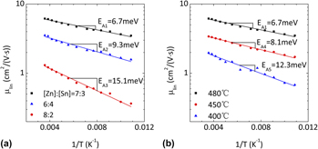
Zinc oxide-based transparent amorphous oxide semiconductors (TAOS) are strong contenders to replace amorphous and polycrystalline silicon for large area display backplanes due to their high electron mobility. To enable future roll-to-roll printed electronics, solution-processed fabrication methods are needed. Here, we use low-temperature measurements from 77 to 300 K to quantitatively compare charge transport mechanisms and band-tail density of states of solution-processed zinc tin oxide (ZTO) thin film transistors fabricated with different film composition and annealing temperature. The devices exhibit percolation conduction with Fermi level pinning at high charge carrier concentrations. The shape and energy levels of band-tail states can be engineered by process and stoichiometry. For optimal amorphous ZTO film with Zn:Sn ink ratio of 7:3 and annealing temperature of 480 °C, the band structure exhibits Arrhenius and percolation energy values of 7 and 3 meV, respectively, better than those measured by others for vacuum-processed TAOS films, showing the potential of solution processing.

Type
Articles
Copyright
Copyright © Materials Research Society 2012

Access options

Get access to the full version of this content by using one of the access options below. (Log in options will check for institutional or personal access. Content may require purchase if you do not have access.)

References

REFERENCES

1.Nomura, K., Ohta, H., Takagi, A., Kamiya, T., Hirano, M., and Hosono, H.: Room-temperature fabrication of transparent flexible thin-film transistors using amorphous oxide semiconductors. Nature 432, 488 (2004).CrossRefGoogle ScholarPubMed
2.Kwon, J.Y., Son, K.S., Jung, J.S., Kim, T.S., Ryu, M.K., Park, K.B., Kim, J.W., Lee, Y.G., Kim, C.J., Kim, S.I., Park, Y.S., Lee, S.Y., and Kim, J.M.: 4 Inch QVGA AMOLED Display Driven by GaInZnO TFT (International Display Workshop, Sapporo, Japan, 2007) p. 1783.Google Scholar
3.Sung, M., Lee, H., Kim, C.N., Kang, S.K., Kim, D.Y., Kim, S., Kim, S.K., Kim, S., Kim, H., and Kim, S.: Novel Backplane for AM-OLED Device (EXCO, Daegu, Korea, 2007) p. 133.Google Scholar
4.Jeong, J.K., Jeong, J.H., Yang, H.W., Ahn, T.K., Kim, M., Kim, K.S., Gu, B.S., Chung, H., Park, J., Mo, Y., Kim, H.D., and Chung, H.K.: 12.1-in. WXGA AMOLED display driven by InGaZnO thin-film transistors. J. Soc. Inf. Disp. 17, 95 (2009).CrossRefGoogle Scholar
5.Ito, M., Kon, M., Miyazaki, C., Ikeda, N., Ishizaki, M., Matsubara, R., Ugajin, Y., and Sekine, N.: Amorphous oxide TFT and their applications in electrophoretic displays. Physica Status Solidi. A Appl. Res. 205, 1885 (2008).CrossRefGoogle Scholar
6.Hong, D., Chiang, H.Q., and Wager, J.F.: Zinc tin oxide thin-film transistors via reactive sputtering using a metal target. J. Vac. Sci. Technol. B Microelectron. Nanometer Struct. Process. Meas. Phenom. 24, L23 (2006).Google Scholar
7.Jackson, W.B., Hoffman, R.L., and Herman, G.S.: High-performance flexible zinc tin oxide field-effect transistors. Appl. Phys. Lett. 87, 193503 (2005).CrossRefGoogle Scholar
8.Görrn, P., Hölzer, P., Riedl, T., Kowalsky, W., Wang, J., Weimann, T., Hinze, P., and Kipp, S.: Stability of transparent zinc tin oxide transistors under bias stress. Appl. Phys. Lett. 90, 063502 (2007).CrossRefGoogle Scholar
9.Chang, Y., Lee, D., Herman, G.S., and Chang, C.: High-performance, spin-coated zinc tin oxide thin-film transistors. Electrochem. Solid-State Lett. 10, H135 (2007).CrossRefGoogle Scholar
10.Jeong, S., Jeong, Y., and Moon, J.: Solution-processed zinc tin oxide semiconductor for thin-film transistors. J. Phys. Chem. C 112, 11082 (2008).CrossRefGoogle Scholar
11.Seo, S., Choi, C.G., Hwang, Y.H., and Bae, B-S.: High performance solution-processed amorphous zinc tin oxide thin film transistor. J. Phys. D: Appl. Phys. 42, 035106 (2009).CrossRefGoogle Scholar
12.Park, S.K., Kim, Y., Kim, H., and Han, J.: High performance solution-processed and lithographically patterned zinc-tin oxide thin-film transistors with good operational stability. Electrochem. Solid-State Lett. 12, H256 (2009).CrossRefGoogle Scholar
13.Kim, D., Jeong, Y., Song, K., Park, S-K., Cao, G., and Moon, J.: Inkjet-printed zinc tin oxide thin-film transistor. Langmuir 25, 11149 (2009).CrossRefGoogle ScholarPubMed
14.Pal, B.N., Dhar, B.M., See, K.C., and Katz, H.E.: Solution-deposited sodium beta-alumina gate dielectrics for low-voltage and transparent field-effect transistors. Nat. Mater. 8, 898 (2009).CrossRefGoogle ScholarPubMed
15.Lee, C. and Dodabalapur, A.: Solution-processed zinc–tin oxide thin-film transistors with low interfacial trap density and improved performance. Appl. Phys. Lett. 96, 243501 (2010).CrossRefGoogle Scholar
16.Kim, Y., Kim, K., Oh, M.S., Kim, H.J., Han, J.I., Han, M., and Park, S.K.: Ink-jet-printed zinc-tin-oxide thin-film transistors and circuits with rapid thermal annealing process. IEEE Electron Device Lett. 31, 836 (2010).Google Scholar
17.Avis, C. and Jang, J.: A high performance inkjet printed zinc tin oxide transparent thin-film transistor manufactured at the maximum process temperature of 300°C and its stability test. Electrochem. Solid-State Lett. 14, J9 (2011).CrossRefGoogle Scholar
18.Shin, J., Hwang, C., Cheong, W., Park, S.K., Cho, D., Ryu, M., Yoon, S., Byun, C., Yang, S., Chu, H.Y., and Cho, K.I.: Analytical modeling of IGZO thin-film transistors based on the exponential distribution of deep and tail state. J. Korean Phys. Soc. 54, 527 (2009).CrossRefGoogle Scholar
19.Fung, T., Chuang, C., Chen, C., Abe, K., Cottle, R., Townsend, M., Kumomi, H., and Kanicki, J.: Two-dimensional numerical simulation of radio frequency sputter amorphous In-Ga-Zn-O thin-film transistors. J. Appl. Phys. 106, 084511 (2009).CrossRefGoogle Scholar
20.Kamiya, T., Nomura, K., and Hosono, H.: Electronic structures above mobility edges in crystalline and amorphous in-Ga-Zn-O: Percolation conduction examined by analytical model. IEEE/OSA J. Disp. Technol. 5, 462 (2009).CrossRefGoogle Scholar
21.Godo, H., Kawae, D., Yoshitomi, S., Sasaki, T., Ito, S., Ohara, H., Kishida, H., Takahashi, M., Miyanaga, A., and Yamazaki, S.: Temperature dependence of transistor characteristics and electronic structure for amorphous in-Ga-Zn-Oxide thin film transistor. Jpn. J. Appl. Phys. 49, 03CB04 (2010).CrossRefGoogle Scholar
22.Kim, C.E., Cho, E.N., Moon, P., Kim, G.H., Kim, D.L., Kim, H.J., and Yun, I.: Density-of-states modeling of solution-processed InGaZnO thin-film transistors. IEEE Electron Device Lett. 31, 1131 (2010).CrossRefGoogle Scholar
23.Jeon, Y.W., Kim, S., Lee, S., Kim, D.M., Kim, D.H., Park, J., Kim, C.J., Song, I., Park, Y., Chung, U., Lee, J., Ahn, B.D., Park, S.Y., Park, J., and Kim, J.H.: Subgap density-of-states-based amorphous oxide thin film transistor simulator (DeAOTS). IEEE Trans. Electron Devices 57, 2988 (2010).CrossRefGoogle Scholar
24.Nomura, K., Kamiya, T., Ohta, H., Ueda, K., Hirano, M., and Hosono, H.: Carrier transport in transparent oxide semiconductor with intrinsic structural randomness probed using single-crystalline InGaO3(ZnO)5 films. Appl. Phys. Lett. 85, 1993 (2004).CrossRefGoogle Scholar
25.Takagi, A., Nomura, K., Ohta, H., Yanagia, H., Kamiya, T., Hirano, M., and Hosono, H.: Carrier transport and electronic structure in amorphous oxide semiconductor, a-InGaZnO4. Thin Solid Films 486, 38 (2005).CrossRefGoogle Scholar
26.Martins, R., Barquinha, P., Pimentel, A., Pereira, L., Fortunato, E., Kang, D., Song, I., Kim, C., Park, J., and Park, Y.: Electron transport in single and multicomponent n-type oxide semiconductors. Thin Solid Films 516, 1322 (2008).CrossRefGoogle Scholar
27.Lee, S., Ghaffarzadeh, K., Nathan, A., Robertson, J., Jeon, S., Kim, C., Song, I., and Chung, U.: Trap-limited and percolation conduction mechanisms in amorphous oxide semiconductor thin film transistors. Appl. Phys. Lett. 98, 203508 (2011).CrossRefGoogle Scholar
28.Lee, C., Cobb, B., and Dodabalapur, A.: Band transport and mobility edge in amorphous solution-processed zinc tin oxide thin-film transistors. Appl. Phys. Lett. 97, 203505 (2010).CrossRefGoogle Scholar
29.Kim, Y., Han, J., and Park, S.K.: Effect of zinc/tin composition ratio on the operational stability of solution-processed zinc–tin–oxide thin-film transistors. IEEE Electron Device Lett. 33, 50 (2012).CrossRefGoogle Scholar
30.Hosono, H., Nomura, K., Ogo, Y., Uruga, T., and Kamiya, T.: Factors controlling electron transport properties in transparent amorphous oxide semiconductors. J. Non-Cryst. Solids 354, 2796 (2008).CrossRefGoogle Scholar
31.Hoffman, R.L.: Effects of channel stoichiometry and processing temperature on the electrical characteristics of zinc tin oxide thin-film transistors. Solid-State Electron. 50, 784 (2006).CrossRefGoogle Scholar
32.Chiang, H.Q., Wager, J.F., Hoffman, R.L., Jeong, J., and Keszler, D.A.: High mobility transparent thin-film transistors with amorphous zinc tin oxide channel layer. Appl. Phys. Lett. 86, 013503 (2005).CrossRefGoogle Scholar
33.Nomura, K., Ohta, H., Ueda, K., Kamiya, T., Hirano, M., and Hosono, H.: Thin-film transistor fabricated in single-crystalline transparent oxide semiconductor. Science 300, 1269 (2003).CrossRefGoogle ScholarPubMed
34.Banger, K.K., Yamashita, Y., Mori, K., Peterson, R.L., Leedham, T., Rickard, J., and Sirringhaus, H.: Low-temperature, high-performance solution-processed metal oxide thin-film transistors formed by a ‘sol–gel on chip’ process. Nat. Mater. 10, 45 (2011).CrossRefGoogle ScholarPubMed
35.Chen, C., Abe, K., Kumomi, H., and Kanicki, J.: Density of states of a-InGaZnO from temperature-dependent field-effect studies. IEEE Trans. Electron Devices 56, 1177 (2009).CrossRefGoogle Scholar
36.Ji, K.H., Kim, J., Jung, H.Y., Park, S.Y., Mo, Y., Jeong, J.H., Kwon, J., Ryu, M., Lee, S.Y., Choi, R., and Jeong, J.K.: The effect of density-of-state on the temperature and gate bias-induced instability of InGaZnO thin film transistors. J. Electrochem. Soc. 157, H983 (2010).CrossRefGoogle Scholar
37.Kaneko, K., Inoue, N., Saito, S., Furutake, N., Sunamura, H., Kawahara, J., Hane, M., and Hayashi, Y.: Highly Reliable BEOL-Transistor with Oxygen-Controlled InGaZnO and Gate/Drain Offset Design for High/Low Voltage Bridging I/O Operations (IEEE International Electron Devices Meeting, Washington, DC, 2011) p. 7.4.1.CrossRefGoogle Scholar
Supplementary material: File

Hu and Peterson supplementary material

Supplementary figures

Download Hu and Peterson supplementary material(File)
File 560.6 KB