


Crossref Citations
This article has been cited by the following publications. This list is generated based on data provided by Crossref.
Kim, Hyuncheol
Choi, Yong-June
Kang, Kyung-Mun
and
Park, Hyung-Ho
2014.
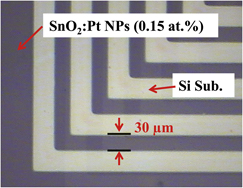
Directly patternable SnO2 thin films incorporating Pt nanoparticles.
Materials Research Bulletin,
Vol. 52,
Issue. ,
p.
6.