Hostname: page-component-7479d7b7d-fwgfc Total loading time: 0 Render date: 2024-07-11T05:18:55.528Z Has data issue: false hasContentIssue false

Atomic layer deposition of epitaxial HfO2 thin films on r-cut sapphire

Published online by Cambridge University Press:  17 May 2013

Hugo Mändar*
Affiliation:
Institute of Physics, University of Tartu, EE-51014 Tartu, Estonia
Raul Rammula
Affiliation:
Institute of Physics, University of Tartu, EE-51014 Tartu, Estonia
Aleks Aidla
Affiliation:
Institute of Physics, University of Tartu, EE-51014 Tartu, Estonia
Jaan Aarik
Affiliation:
Institute of Physics, University of Tartu, EE-51014 Tartu, Estonia
*
a)Address all correspondence to this author. e-mail: hugo.mandar@ut.ee
Get access

Abstract

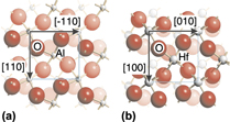
Textured epitaxial HfO2 thin films of monoclinic structure were grown on r-cut Al2O3 by atomic layer deposition from HfCl4 and H2O at temperatures 450–750 °C. The film-to-substrate out-of-plane orientation was determined to have a single (001)HfO2//(1$\bar 1$02)α-Al2O3 relationship. The in-plane orientation showed the existence of two possible relationships: [100]HfO2//[110]α-Al2O3 and [$\bar 1$00]HfO2//[110]α-Al2O3. In films deposited at 400 °C traces of (010) growth plane were observed in addition to the preferential (001) growth. The lattice of HfO2 was compressed in the surface plane and expanded in the surface normal direction. The strain was highest in the films grown at 450–550 °C. With the increase of deposition temperature to 750 °C, the strain decreased. The strain relaxation in films deposited at 750 °C was in correlation with marked surface roughening in the initial stage of deposition at this temperature. The roughness of the epitaxial films was lower than that of polycrystalline films with comparable thickness deposited on Si(100) and SiO2 substrates.

Type
Articles
Copyright
Copyright © Materials Research Society 2013 

Access options

Get access to the full version of this content by using one of the access options below. (Log in options will check for institutional or personal access. Content may require purchase if you do not have access.)

References

REFERENCES

Park, K-Y., Cho, H-I., Choi, H-C., Bae, Y-H., Lee, C-S., Lee, J-L., and Lee, J-H.: Device characteristics of AlGaN/GaN MIS-HFET using Al2O3–HfO2 laminated high-k dielectric. Jpn. J. Appl. Phys. 43(11A), L1433 (2004).CrossRefGoogle Scholar
Deen, D.A., Binari, S.C., Storm, D.F., Katzer, D.S., Roussos, J.A., Hackley, J.C., and Gougousi, T.: AlN/GaN insulated gate HEMTs with HfO2 gate dielectric. Electron. Lett. 45(8), 423 (2009).CrossRefGoogle Scholar
Choi, J.H., Mao, Y., and Chang, J.P.: Development of hafnium based high-k materials—A review. Mater. Sci. Eng., R 72, 97 (2011).CrossRefGoogle Scholar
Sriraman, V., Li, X., Singh, N., and Lee, S.: HfO2-based RRAM devices with varying contact sizes and their electrical behavior. IEEE Electron Device Lett. 33, 1060 (2012).CrossRefGoogle Scholar
Ye, Z-H., Chang-Liao, K-S., Tsai, C-Y., Tsai, T-T., and Wang, T-K.: Enhanced operation in charge-trapping non-volatile memory device with Si3N4/Al2O3/HfO2 carge trapping layer. IEEE Electron Device Lett. 33, 1351 (2012).CrossRefGoogle Scholar
Hamden, E.T., Greer, F., Hoenk, M.E., Blacksberg, J., Dickie, M.R., Nikzad, S., Martin, D.C., and Schiminovich, D.: Ultraviolet antireflection coatings for use in silicon detector design. Appl. Opt. 50(21), 4180 (2011).CrossRefGoogle ScholarPubMed
Chen, S., Zhao, Y., Yu, Z., Fang, Z., Li, D., He, H., and Shao, J.: Femtosecond laser-induced damage of HfO2/SiO2 mirror with different stack structure. Appl. Opt. 51(25), 6188 (2012).CrossRefGoogle ScholarPubMed
Concalves, R.R., Carturan, G., Montagna, M., Ferrari, M., Zampedri, L., Pelli, S., Righini, G.C., Ribeiro, S.J.L., and Messaddeq, Y.: Erbium-activated HfO2–based waveguides for photonics. Opt. Mater. 25, 131 (2004).CrossRefGoogle Scholar
Mitchell, D.R.G., Aarik, J., and Aidla, A.: Transmission electron microscopy studies of HfO2 thin films grown by chloride-based atomic layer deposition. Appl. Surf. Sci. 253, 606 (2006).CrossRefGoogle Scholar
Fröhlich, K., Aarik, J., Ťapajna, M., Rosová, A., Aidla, A., Dobročka, E., and Hušeková, K.: Epitaxial growth of high-k TiO2 rutile films on RuO2 electrodes. J. Vac. Sci. Technol., B 27(1), 266 (2009).CrossRefGoogle Scholar
Dai, J.Y., Lee, P.F., Wong, K.H., Chan, H.L.W., and Choy, C.L.: Epitaxial growth of yttrium-stabilized HfO2 high-k gate dielectric thin films on Si. J. Appl. Phys. V94(2), 912 (2003).CrossRefGoogle Scholar
Yang, Z.K., Lee, W.C., Lee, Y.J., Chang, P., Huang, M.L., Hong, M., Yu, K.L., Tang, M-T., Lin, B-H., Hsu, C-H., and Kwo, J.: Structural and compositional investigation of yttrium-doped HfO2 films epitaxially grown on Si(111). Appl. Phys. Lett. 91, 202909 (2007).CrossRefGoogle Scholar
Zhang, X., Tu, H., Wei, F., Wang, L., and Du, J.: Cube-on-cube epitaxy of Gd2O3-doped HfO2 films on Si(100) substrates by pulse laser deposition. J. Cryst. Growth 312, 41 (2009).CrossRefGoogle Scholar
Zhang, X., Tu, H., Wang, X., Xiong, Y., Yang, M., Wang, L., and Du, J.: Hetero-epitaxial growth of the cubic single crystalline HfO2 film as high-k materials by pulsed laser ablation. J. Cryst. Growth 312, 2928 (2010).CrossRefGoogle Scholar
Gusev, E.P., Shang, H., Copel, M., Gribelyuk, M., D’Emic, C., Kozlowski, P., and Zabel, T.: Microstructure and thermal stability of HfO2 gate dielectric deposited on Ge(100). Appl. Phys. Lett. 85(12), 2334 (2004).CrossRefGoogle Scholar
Delabie, A., Puurunen, R.L., Brijs, B., Caymax, M., Conard, T., Onsia, B., Richard, O., Vandervorst, W., Zhao, C., Heyns, M.M., Meuris, M., Viitanen, M.M., Brongersma, H.H., de Ridder, M., Goncharova, L.V., Garfunkel, E., Gustafsson, T., and Tsai, W.: Atomic layer deposition of hafnium oxide on germanium substrates. J. Appl. Phys. 97, 064104 (2005).CrossRefGoogle Scholar
Hsu, C-H., Chang, P., Lee, W.C., Yang, Z.K., Lee, Y.J., Hong, M., Kwo, J., Huang, C.M., and Lee, H.Y., Structure of HfO2 films epitaxially grown on GaAs(001). Appl. Phys. Lett. 89, 122907 (2006).CrossRefGoogle Scholar
Liou, S.C., Chu, M-W., Chen, C.H., Lee, Y.J., Chang, P., Lee, W.C., Hong, M., and Kwo, J.: Transmission electron microscopy characterization of HfO2/GaAs(001) heterostructures grown by molecular beam epitaxy. Appl. Phys. A 91, 585 (2008).CrossRefGoogle Scholar
Forsgren, K., Hårsta, A., Aarik, J., Aidla, A., Westlinder, J., and Olsson, J.: Deposition of HfO2 thin films in HfI4-based processes. J. Electrochem. Soc. 149, F139 (2002).CrossRefGoogle Scholar
Bagmut, A.G., Bagmut, I.A., Zhuchkov, V.A., and Shevchenko, M.O.: Phase transformations in films deposited by laser ablation of Hf in an oxygen atmosphere. Technol. Phys. 57(6), 856 (2012).CrossRefGoogle Scholar
Asaoka, H., Katano, Y., and Noda, K.: Epitaxial growth of zirconium dioxide films on sapphire substrates. Appl. Surf. Sci. 113114, 198 (1997).CrossRefGoogle Scholar
Schuisky, M., Hårsta, A., Aidla, A., Kukli, K., Kiisler, A-A., and Aarik, J.: Atomic layer chemical vapor deposition of TiO2: Low temperature epitaxy of rutile and anatase. J. Electrochem. Soc. 147, 3319 (2000).CrossRefGoogle Scholar
Tarre, A., Rosental, A., Aidla, A., Aarik, J., Sundqvist, J., and Hårsta, A.: New routes to SnO2 heteroepitaxy. Vacuum 76, 571 (2002).CrossRefGoogle Scholar
Lie, M., Fjellvag, H., and Kjekshus, A.: Growth of Fe2O3 thin films by atomic layer deposition. Thin Solid Films 488, 74 (2005).CrossRefGoogle Scholar
Mändar, H., Uustare, T., Aarik, J., Tarre, A., and Rosental, A.: Characterization of asymmetric rhombohedral twin in epitaxial α-Cr2O3 thin films by X-ray and electron diffraction. Thin Solid Films 515, 4570 (2007).CrossRefGoogle Scholar
Ribeiro, S.J.L., Messaddeq, Y., Goncalves, R.R., Ferrari, M., Montagna, M., and Aegerter, M.A.: Low optical loss planar waveguides prepared in an organic–inorganic hybrid system. Appl. Phys. Lett. 77, 3502 (2000).CrossRefGoogle Scholar
Aslan, M.M., Webster, N.A., Byard, C.L., Pereira, M.B., Hayes, C.M., Wiederkehr, R.S., and Mendes, S.B.: Low-loss optical waveguides for the near ultra-violet and visible spectral regions with Al2O3 thin films from atomic layer deposition. Thin Solid Films 518, 4935 (2010).CrossRefGoogle ScholarPubMed
Mroczyński, R., Taube, A., Gierałtowska, S., Guziewicz, E., and Godlewski, M.: Application of deposited by ALD HfO2 and Al2O3 layers in double-gate dielectric stacks for non-volatile semiconductor memory (NVSM) devices. Appl. Surf. Sci. 258, 8366 (2012).CrossRefGoogle Scholar
Lee, W.C., Chin, B.H., Chu, L.K., Lin, T.D., Lee, Y.J., Tung, L.T., Lee, C.H., Hong, M., and Kwob, J.: Molecular beam epitaxy-grown Al2O3/HfO2 high-k dielectrics for germanium. J. Cryst. Growth 311, 2187 (2009).CrossRefGoogle Scholar
Lee, C., Choi, J., Cho, M., Park, J., Hwang, C.S., and Kim, H.J.: Nitrogen incorporation engineering and electrical properties of high-k gate dielectric (HfO2 and Al2O3) films on Si (100) substrate. J. Vac. Sci. Technol., B 22, 1838 (2004).CrossRefGoogle Scholar
Aarik, J., Aidla, A., Kiisler, A-A., Uustare, T., and Sammelselg, V.: Influence of substrate temperature on atomic layer growth and properties of HfO2 thin films. Thin Solid Films 340, 110 (1999).CrossRefGoogle Scholar
Aarik, J., Aidla, A., Mändar, H., Sammelselg, V., and Uustare, T.: Texture development in nanocrystalline hafnium dioxide thin films grown by atomic layer deposition. J. Cryst. Growth 220, 105 (2000).CrossRefGoogle Scholar
Trainor, T.P., Eng, P.J., Brown, G.E. Jr., Robinson, I.K., and De Santis, M.: Crystal truncation rod diffraction study of the α-Al2O3(1 $\bar 1$02) surface. Surf. Sci. 496, 238 (2002).CrossRefGoogle Scholar
Macrae, C.F., Bruno, I.J., Chisholm, J.A., Edgington, P.R., McCabe, P., Pidcock, E., Rodriguez-Monge, L., Taylor, R., van de Streek, J., and Wood, P.A.: Mercury CSD 2.0-new features for the visualization and investigation of crystal structures. J. Appl. Cryst. 41, 466 (2008).CrossRefGoogle Scholar
Daudin, B., Widmann, F., Feuillet, G., Samson, Y., Arlery, M., and Rouviere, J.L.: Stranski-Krastanov growth mode during the molecular beam epitaxy of highly strained GaN, Phys. Rev. B 56, R7069 (1997).CrossRefGoogle Scholar
Rammula, R., Aarik, J., Mändar, H., Ritslaid, P., and Sammelselg, V.: Atomic layer deposition of HfO2: Effect of structure development on growth rate, morphology and optical properties of thin films. Appl. Surf. Sci. 257(3), 1043 (2010).CrossRefGoogle Scholar
Aarik, J., Aidla, A., Kikas, A., Käämbre, T., Rammula, R., Ritslaid, P., Uustare, T., and Sammelselg, V.: Effects of precursors on nucleation in atomic layer deposition of HfO2. Appl. Surf. Sci. 230, 292 (2004).CrossRefGoogle Scholar