


I. INTRODUCTION
A Resistive Random Access Memory (ReRAM) possesses a variety of great potential as a next-generation nonvolatile memory. Reference Baek, Lee, Seo, Lee, Seo, Suh, Park, Park, Kim, Yoo, Chung and Moon1–Reference Pan, Gao, Chen, Song and Zeng4 A key phenomenon behind ReRAMs is a resistive switching (RS). RS mechanism in ReRAM especially based on binary transition metal oxide (TMO) cells has been explained by the formation and rupture of conductive filaments. This reversible resistance transition by applying repeated electrical stress between the low-resistance state (LRS) and the high-resistance state (HRS) can occur after an initial operation “forming” process to an initial cell to create conductive filaments in TMO layers between top and bottom metal electrodes. The conductive filaments are believed to be composed of oxygen vacancies Reference Akinaga and Shima3,Reference Waser and Aono5,Reference Waser, Dittmann, Staikov and Szot6 or cation interstitials, Reference Valov, Waser, Jameson and Kozicki7–Reference Lu, Jeong, Kozicki and Waser9 which result in the change of microscopic oxygen stoichiometry and the associated formation of point defects in the TMO layers. The oxygen vacancies or cation interstitials typically act as mobile donors because the migration of a negatively charged oxygen ion from the oxygen lattice site creates a positive charge according to charge neutrality condition. In particular, RS memories based on the migration of nanoscale ions and a redox reaction are named as valence change memories (VCMs) after this valence change. Reference Waser, Dittmann, Staikov and Szot6 The voltage polarities between the transition from HRS to LRS (Set) and that from LRS to HRS (Reset) are opposite in VCMs. In other specific TMO-based RS cells, RS behaviors are, however, not dominated by the migration of oxygen ions but by thermally controlled diffusion and a redox reaction. These RS memories are categorized into thermochemical memories (TCMs). Reference Ielmini, Bruchhaus and Waser10 TCMs exhibit uni-polar RS behaviors which means that the voltage polarities between Set and Reset are the same, as opposed to bi-polar RS behaviors in VCMs. On the other hand, RS memories consisting of both one active (oxidizable) electrode such as Ag or Cu and the counter inert electrode such as Pt or TiN are widely known as conductive bridging random access memories (CBRAMs). Reference Gopalan, Ma, Gallo, Wang, Runnion, Saenz, Koushan, Blanchard and Hollmer11 When a positive voltage is applied to the active electrode, dissolution and ionization of the active metal and bridging of a metallic conductive filament to the opposite inert electrode through the TMO layer. The metal ions move toward the active electrode and the filament is eventually ruptured by application of a negative voltage to the active electrode. This kind of memories is called as electrochemical metallization memory (ECM) Reference Ielmini, Bruchhaus and Waser10 owing to these electrochemical processes. ECMs show only bi-polar RS behaviors.
When the scale of the weakest spot in conductive filaments becomes an atomic contact size, conductance quantization is expected to appear. In recent years, observation of quantized conductance discrete steps characterized by integer or half integer multiples of G 0 = 2e 2/h has been reported in ECMs Reference Tsuruoka, Hasegawa, Terabe and Aono8,Reference Tappertzhofen, Valov and Waser12–Reference Lv, Xu, Sun, Liu, Luo, Liu, Banerjee, Sun, Long, Li and Liu18 and VCMs. Reference Miranda, Kano, Dou, Kakushima, Suñé and Iwai19–Reference Syu, Chang, Lou, Tsai, Chang, Tsai, Wang, Liu and Sze23 While there is a few studies on the conductance quantization effect in TCMs, Reference Zhu, Su, Liu, Hu, Pan, Lu, Zhang and Li14,Reference Long, Lian, Cagli, Cartoixà, Rurali, Miranda, Jimenez, Perniola, Liu and Suñé24 we have reported that a conductive filament including a quantum point contact (QPC) can be formed in Pt/NiO/Pt RS cells. Reference Sasakura, Nishi and Kimoto25 Fig. 1 shows two different modes of forming processes by initial voltage sweeping in the cells. Two abrupt current jumps can be observed in Fig. 1(b). The first step is referred to as “semiforming”, and the second step as “second forming”. Conductance quantization occurs between semiforming and second forming as shown in Fig. 1(c). In addition, we have confirmed two different RS behaviors both after semiforming under small compliance current (I comp.) shown in Fig. 1(a), and after second forming under large compliance current shown in Fig. 1(b). This is why these steps can be referred as kinds of forming processes. Two kinds of forming and nonpolar (both uni-polar and bi-polar) RS characteristics are unique phenomena even in TCMs. Furthermore, the filament including a QPC created by semiforming turned out to be possibly sensitive to just heat not Joule heating. Reference Sasakura, Nishi and Kimoto25

FIG. 1. Two different modes of forming processes and subsquent RS characteristics in Pt/NiO/Pt cells. RS behavior (a) after semiforming and (b) after second forming. (c) G/G 0 − V characteristics between semiforming and second forming in (a).
In this study, we studied the appearance condition of conductance quantization in the Pt/NiO/Pt cells. The condition is equivalent to the appearance of two kinds of forming, especially semiforming. Investigation of the condition contributes to clarify the possible source and distributions of a filament including a QPC. Dependences of both forming characteristics and composition ratio of O to Ni in NiO layers on fabrication process parameters have been investigated. Distribution of microscopic oxygen stoichiometry and the possible source of point defects in the NiO layers was revealed by Transmission Electron Microscopy (TEM) analyses. Moreover, the composition ratio dependence of semiforming voltage indicates the correlation between the oxygen stoichiometry of the weakest spot in conductive filaments and O2 flow rate during NiO deposition by reactive sputtering. Finally, the RS model with conductance quantization was also discussed. These results enable to distinguish the driving force of reset in TCMs in the future.
II. EXPERIMENTAL
Capacitor-type Pt/NiO/Pt RS samples were fabricated as follows. A Pt bottom electrode was deposited by dc sputtering on a SiO2/p-Si substrate inserted by a Ti adhesion layer. The thickness of the Pt bottom electrode was 80 nm. A NiO film as a resistance change layer was subsequently deposited by radio-frequency reactive sputtering in Ar and O2 gas mixture using a metallic Ni target. The O2 flow rate was precisely controlled because electrical properties in Pt/NiO/Pt cells are sensitive to oxygen composition in a NiO layer. Reference Sasakura, Nishi and Kimoto25,Reference Nishi, Iwata and Kimoto26 The pressure and the substrate temperature during sputtering were kept at 0.6 Pa and 350 °C, respectively. The thickness of the NiO film was 80 nm. Pt top electrodes with a diameter of 100 μm were deposited on the NiO layer by electron beam evaporation through a metal shadow mask. The Pt/NiO/Pt cell size is determined by the area of the top electrode. Figure 2 shows a cross-sectional TEM image of a typical capacitor-type Pt/NiO/Pt stack. The image revealed that a NiO layer exhibits a columnar polycrystalline structure with a grain diameter of tens of nanometer scale. Note that roughly all of grain boundaries run along the thickness direction.

FIG. 2. Cross-sectional TEM image of a planar-type Pt/NiO/Pt cell.
Crossbar-type Pt/NiO/Pt RS samples were also fabricated to investigate the cell size dependence of forming characteristics. The Pt/NiO/Pt cells were directly sandwiched between bar-shape top and bottom electrodes selectively formed by UV photolithography. The Pt top electrodes of cells were separated from each other to avoid a sneak-path problem. Reference Flocke and Noll27,Reference Linn, Rosezin, Kugeler and Waser28 The deposition conditions of Pt bottom electrodes and a NiO layer were as same as capacitor-type samples. The thickness of the Pt top and bottom electrodes was approximately 50 nm. Pt top electrodes were deposited on the NiO layer by dc sputtering. The cell size is equivalent to the cross-point area, which falls under any of 4 × 4, 20 × 20, and 88 × 88 μm2 in this study. The structure of NiO layer is the same columnar polycrystalline as capacitor-type samples.
A Pt bottom electrode was grounded and voltage was applied to a Pt top electrode. Forming characteristics of the cells were measured in a voltage-sweep mode at room temperature using a Keithley 4200 Semiconductor Parameter Analyzer (Tektoronix, Cleveland, Ohio). Average forming voltage of cells exhibited large variation. Most of the cells in all the samples were confirmed to exhibit nonpolar RS characteristics after any forming processes.
III. RESULTS AND DISCUSSION
A. O2 flow rate and cell size dependences of forming characteristics
Figure 3 exhibits dependence of forming characteristics in capacitor-type samples on O2 flow rate during NiO deposition by reactive sputtering. The varied range of O2 flow rate is less than 5% of the middle. The values of O2 flow rate in Figs. 3(a)–3(c) are 0.94 sccm, 0.96 sccm, and 0.98 sccm, respectively, in the case that the Ar flow rate is 7.8 sccm. When the O2 flow rate is relatively low, forming does not occur below a compliance current (10 mA) because of initial low resistance (nonforming) as shown in Fig. 3(a). On the other hand, the cells fabricated with a higher O2 flow rate tend to show only single forming, which corresponds to conventional forming characteristics as shown in Fig. 3(c). As a result, when the NiO layer is deposited with a selected O2 flow rate, conductance quantization appears between semiforming and second forming as shown in Fig. 3(b). Reference Sasakura, Nishi and Kimoto25

FIG. 3. O2 flow rate dependence of forming characteristics in capacitor-type Pt/NiO/Pt cells. The O2 flow rate gradually increases from (a) to (c).
Figure 4 shows plane-view High-Angle Annular Dark Field (HAADF) Scanning TEM (STEM) images taken at NiO deposited with different O2 flow rates. These images were selected at the regions without Pt top electrodes. Furthermore, backside materials (Pt bottom electrode and a substrate) in samples were completely removed for the TEM observation to acquire the intrinsic signals only from the NiO layers. As the O2 flow rate becomes lower, more bright spots appeared in the images as shown in Fig. 4(a). The magnified image near bright spots shown in Fig. 5(a) reveals that the bright spots can be observed at grain boundaries, and more specifically frequently at grain boundary triple-points. Figures 5(b) and 5(c) are Energy Dispersive X-ray (EDX) mapping images of O and Ni signals corresponding to the area shown in Fig. 5(a), respectively. These maps revealed that the bright spots in HAADF images indicate oxygen vacancy (V O)-rich and Ni-rich grain boundaries. Because brightness of the spots in Fig. 5(a) means the average composition ratio of O to Ni along the thickness direction, the ratio at the triple-points is smaller than the value within grains. These results suggest that O desorbs from the grain boundaries more easily than from other regions within grains during NiO deposition because of difference of their surface energies. As the O2 flow rate becomes lower, V O-rich grain boundaries generate an extremely low O/Ni composition ratio at grain boundary triple-points, which correspond to bright spots in HAADF images. However, it is difficult to determine whether the origin of bright spots is a row of V Os or segregated Ni atoms in this study. For simplicity, we hereafter proceed discussion in terms of the number of V Os as a source of composition distribution instead of excess Ni atoms. As a consequence, V Os are randomly distributed at grain boundaries, especially triple points, as a function of brightness in HAADF images. As the O2 flow rate becomes lower, the number of V O-rich grain boundaries increases, as expected.

FIG. 4. Plane-view HAADF STEM images taken at only NiO deposited with different O2 flow rates in capacitor-type Pt/NiO/Pt samples. The O2 flow rate gradually increases from (a) to (c).

FIG. 5. Bright spots at grain-boundary, especially triple-points, in (a) HAADF-STEM image indicated (b) V O-rich (O-deficient) and (c) Ni-rich regions in EDX maps of oxygen and nickel signals, respectively.
Next, we investigated cell size dependence of forming characteristics in crossbar-type samples, in which NiO layers were deposited by reactive sputtering with different O2 flow rates. Figure 6 exhibits dominant forming characteristics in each cell with a size of (a) 4 × 4 μm2, (b) 20 × 20, and (c) 88 × 88 μm2. The values of Ar and O2 flow rate are 7.8 sccm and 0.94 sccm, respectively. Figure 6(b) shows two modes of forming processes and conductance quantization between semiforming and second forming. When the cell size becomes small, the cells tend to exhibit single forming, which is similar to the forming characteristics shown in Fig. 3(c). Although the cell size and initial resistance are different with those of the cells in Fig. 3, this forming characteristic is equivalent to that shown in Fig. 3(c). On the other hand, forming does not occur because of initial low resistance as the cell size becomes larger as shown in Fig. 6(c). These results suggest that magnitude relationship of Pt/NiO/Pt cell size is the same as that of V O-rich grain boundaries in NiO layers.

FIG. 6. Cell size dependence of forming characteristics in crossbar-type Pt/NiO/Pt cells. The cell size is (a) 4 × 4 μm2, (b) 20 × 20 μm2, and (c) 88 × 88 μm2.
B. RS model
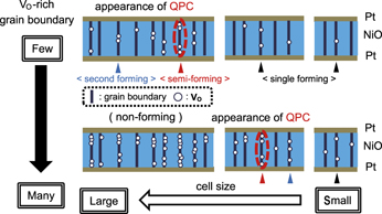
We discuss the appearance condition of QPC based on experimental tendency of forming characteristics described above. Figure 7 illustrates the schematics of a proposed RS model. When too many V Os are present along a grain boundary in a NiO layer, the initial resistance of a cell is low and it is hard to observe the forming (nonforming). This kind of cell should be excluded to consider the proposed RS model because forming does not occur. Here, the number of V Os in all of grain boundaries in a cell, which exhibits a low initial resistance, is assumed to be larger than 4 in Fig. 7. When voltage is swept to the initial cells, semiforming occurs and a conductive filament including a QPC is formed at the weakest V O-rich grain boundary (with the maximum number of V Os), in which “moderate” number of V Os are included (the number is assumed to be 4 in Fig. 7). If voltage sweeping is stopped just after semiforming, re-application of voltage results in reset and set occurs alternately as shown in Fig. 1(a), which means the rupture and formation of the conductive filament including a QPC. Upon the application of higher voltage after semiforming, the conductive filament including a QPC begins to be fat step by step according to conductance quantization. Further voltage application brings about second forming by creating a new fat conductive filament at one of other weak grain boundaries not by changing of a filament including a QPC to much fatter filament. In the case that a “moderate” V O-rich grain boundary does not exist in the cell (the number is assumed to be <4 in Fig. 7), only single forming occurs in the same manner. After second forming or single forming, a RS behavior is observed by the rupture and formation of a new fat filament as shown in Fig. 1(b) because the resistance in the HRS just after large current through a higher-conductive filament followed by reset is nearly identical to the resistance just after second forming instead of the initial resistance, although the filaments including a QPC are possibly ruptured by heat of even 370 K. Reference Sasakura, Nishi and Kimoto25

FIG. 7. Schematics of a proposed resistive switching (RS) model. When voltage is swept to the initial cells, semiforming occurs and a conductive filament including a QPC is formed at the weakest V O-rich grain boundary (red marked). Further voltage application brings about second forming by creating a new fat conductive filament at one of other weak V O-rich grain boundaries (blue marked). In the case that a “moderate” V O-rich grain boundary does not exist in the cell, only single forming occurs and a fat conductive filament at the weakest V O-rich grain boundary is formed (black marked).
These results indicate that the maximum number of V Os in a grain boundary is a key parameter. Too-rich or too-poor V Os results in nonforming or single forming, respectively. In summary, the appearance condition of QPC in a Pt/NiO/Pt cell is existence of “moderate” V O-rich grain boundary in a NiO layer.
C. Appearance or disappearance of QPC
The physical meaning of semi-forming voltage (V s-form) is of importance for considering appearance of QPC. Figure 8 shows typical forming characteristics in capacitor-type samples deposited with slightly different O2 flow rates, which exhibit two modes of forming processes or single forming. Figures 8(a) and 8(c) are previously shown as Figs. 3(b) and 3(c), respectively. The values of O2 flow rate in Figs. 8(a)–8(c) are 0.96 sccm, 0.97 sccm, and 0.98 sccm, respectively, in the case that the Ar flow rate is 7.8 sccm. As the O2 flow rate increase, that is, “moderate” V O-rich grain boundary density becomes lower, average V s-form gradually increases and finally a cell exhibits only single forming. The relationship of Pt/NiO/Pt cell size and the number of V Os in grain boundaries in a NiO layer as described above revealed that decrease in density of “moderate” V O-rich grain boundary D or cell size A leads to increase in V s-form, which means fewer occurrence of semiforming and appearance of QPC.

FIG. 8. Forming characteristics in capacitor-type samples deposited with slightly different O2 flow rates, which exhibit two modes of forming processes or single forming. The O2 flow rate gradually increases from (a) to (c).
Forming process in ReRAM cells can be often compared with SiO2 soft breakdown in MOS structures. Reference Akinaga and Shima3,Reference Luo, Liu, Feng, Lin, Huang, Lin and Hou29–Reference Nishi and Kimoto31 The breakdown follows the weakest link theory based on a percolation model, where percolation paths thorough SiO2 thin films are formed by defects due to electrical stress. Reference Degraeve, Ogier, Bellens, Roussel, Groeseneken and Maes32–Reference Wu and Suñé34 Because the defects are randomly distributed according to Poisson statistics, the cumulative breakdown probability F is described as follows Reference Nishi and Kimoto31,Reference Wu and Vollertsen35 :
 $$F = 1 - \exp \left( { - DA} \right)\quad ,$$
where D is the defect density in a SiO2 layer and A is a cell size. When F and D are replaced by the cumulative semiforming probability and “moderate” V O-rich grain boundary density, respectively, Eq. (1) supports the cell size dependence of the semiforming characteristics as shown in Fig. 7. As density of “moderate” V O-rich grain boundary becomes lower, the value of F approaches from 1 to 0. F = 0 means disappearance of QPC and only single forming is observed. Our experimental results as shown in Figs. 6 and 8 indicate that “moderate” V O-rich grain boundaries which act as the source of a filament including a QPC by semiforming may be randomly distributed in a NiO layer according to Poisson statistics.
IV. CONCLUSIONS
Two kinds of forming processes and nonpolar RS characteristics were observed in Pt/NiO/Pt RS cells, in which NiO layers were deposited by reactive sputtering with a selected O2 flow rate. We investigate the O2 flow rate and cell size dependences of forming characteristics and the composition ratio of O to Ni in NiO layers. TEM-EDX maps revealed that the ratio at grain boundaries, especially triple points, is either equal to or clearly smaller than the value within grains. Too-rich or too-poor V Os in grain boundaries results in disappearance of QPC because of nonforming or single forming characteristics, respectively. Because V O-rich weak spots may be randomly distributed at grain boundary triple-points according to Poisson statistics, the cell size dependence of forming characteristics is well explained by the area scaling law. The appearance condition of QPC in a Pt/NiO/Pt cell is existence of “moderate” V O-rich grain boundary in a NiO layer.
Furthermore, we proposed a RS model based on forming characteristics especially obtained from the RS cells with different size. When voltage is swept to the initial cells, semiforming occurs and a conductive filament including a QPC is formed at the weakest V O-rich grain boundary. Further voltage application brings about second forming by creating a new fat conductive filament at one of other weak V O-rich grain boundaries. After both semiforming and second forming, nonpolar RS behaviors occur by the rupture and formation of both a conductive filament including a QPC and a new fat filament, respectively.


