


1 Introduction
Potassium dihydrogen phosphate (KDP) and its deuterated analog, potassium dideuterium phosphate (DKDP) crystals are remarkable multifunctional crystal materials, which are widely applied in fields such as frequency conversion, electro-optic modulation and optical rapid switches[Reference Eimerl1]. However, the crystal performance is limited due to the unwanted optical absorption, which is attributed to point defects created during crystal growth or generated by irradiation[Reference Davis, Hughes and Lee2–Reference Ogorodnikov, Yakovlev, Shul’gin and Satybaldieva7]. Understanding the role played by point defects in bulk crystals has been a subject of great interest and importance for improving quality and performance of the material[Reference Wang, Fang, Zhang, Liu, Boughton, Wang and Zhao8, Reference Liu, Kioussis, Demos and Radousky9]. Several theoretical and experimental studies have suggested that point defects in bulk crystals can provide states in the band gap[Reference Wang, Fang, Zhang, Liu, Boughton, Wang and Zhao8–Reference Liu, Hou, Kioussis, Demos and Radousky11] and assist in the multiphoton absorption process[Reference Carr, Radousky and Demos12–Reference Duchateau, Geoffroy, Belsky, Fedorov, Martin and Guizard16].
Throughout the literature, some models have been proposed for understanding the effect of defect states on the nonlinear absorption (NLA) properties of KDP/DKDP crystals. Demos et al. proposed that defects induced two electronic states in the band gap that facilitated excitation of valence electrons to the conduction band (CB) through sequential one-photon absorption events at 355 nm and (
 $1+2+1$
)-photon absorption (PA) at 532 nm[Reference Demos, DeMange, Negres and Feit13]. Duchateau et al. also developed a model with two defect states in the band gap, which reduced the order of the multiphoton process to interpret the physical mechanisms of two relaxation dynamics in the KDP/DKDP crystals at 800 nm[Reference Duchateau, Geoffroy, Dyan, Piombini and Guizard14]. However, defect states located in the band gap may change under laser irradiation since they can be produced or eliminated with the addition or removal of electrons[Reference Wang, Fang, Zhang, Liu, Boughton, Wang and Zhao8–Reference Liu, Hou, Kioussis, Demos and Radousky11] and subsequently induce changes in the NLA properties of KDP/DKDP crystals[Reference Davis, Hughes and Lee2–Reference Demos, Staggs and Radousky4]. The NLA properties of DKDP crystals have been characterized by some authors with the picosecond Z-scan method[Reference Wang, Wang, Wang, Shen, Li, Huang, Liu and Boughton17, Reference Wang, Li, Wang, Wang, Shen, Ding, Li, Huang and Lu18]. However, these experiments were performed under low laser irradiation intensities. In this work, we have carried out studies on the NLA properties of DKDP crystals in the sub-picosecond time scale, allowing us to perform Z-scan experiments with much higher laser intensities and observe possible changes. A model based on the change of multiphoton absorption mechanism induced by the transformation of defect species is proposed to interpret the experimental data.
$1+2+1$
)-photon absorption (PA) at 532 nm[Reference Demos, DeMange, Negres and Feit13]. Duchateau et al. also developed a model with two defect states in the band gap, which reduced the order of the multiphoton process to interpret the physical mechanisms of two relaxation dynamics in the KDP/DKDP crystals at 800 nm[Reference Duchateau, Geoffroy, Dyan, Piombini and Guizard14]. However, defect states located in the band gap may change under laser irradiation since they can be produced or eliminated with the addition or removal of electrons[Reference Wang, Fang, Zhang, Liu, Boughton, Wang and Zhao8–Reference Liu, Hou, Kioussis, Demos and Radousky11] and subsequently induce changes in the NLA properties of KDP/DKDP crystals[Reference Davis, Hughes and Lee2–Reference Demos, Staggs and Radousky4]. The NLA properties of DKDP crystals have been characterized by some authors with the picosecond Z-scan method[Reference Wang, Wang, Wang, Shen, Li, Huang, Liu and Boughton17, Reference Wang, Li, Wang, Wang, Shen, Ding, Li, Huang and Lu18]. However, these experiments were performed under low laser irradiation intensities. In this work, we have carried out studies on the NLA properties of DKDP crystals in the sub-picosecond time scale, allowing us to perform Z-scan experiments with much higher laser intensities and observe possible changes. A model based on the change of multiphoton absorption mechanism induced by the transformation of defect species is proposed to interpret the experimental data.
2 Experimental setup
The NLA properties of the samples were investigated by an open-aperture (OA) Z-scan system[Reference Sheik-Bahae, Said, Wei, Hagan and Van Stryland19–Reference Wang, Wang, Fan, Lotya, O’Neill, Fox, Feng, Zhang, Jiang, Zhao, Zhang, Coleman, Zhang and Blau21]. The pump source of the Z-scan system was a mode-locked fiber laser with a wavelength of 1030 nm (pulse duration of 340 fs and repetition rate of 1 kHz). The NLA of the sample was investigated at a second harmonic wavelength, 515 nm, with a photon energy
 $\hslash \unicode[STIX]{x1D714}=2.41~\text{eV}$
. The pump beam was focused on the sample with a minimum beam waist radius of
$\hslash \unicode[STIX]{x1D714}=2.41~\text{eV}$
. The pump beam was focused on the sample with a minimum beam waist radius of
 ${\sim}12.5~\unicode[STIX]{x03BC}\text{m}$
through a lens with a focal length of 15 cm. The sample investigated in this study was a type-II cut DKDP crystal (70% deuteration level) grown by the conventional method. The sample was cut into
${\sim}12.5~\unicode[STIX]{x03BC}\text{m}$
through a lens with a focal length of 15 cm. The sample investigated in this study was a type-II cut DKDP crystal (70% deuteration level) grown by the conventional method. The sample was cut into
 $30~\text{mm}\times 30~\text{mm}\times 0.5~\text{mm}$
dimensions and polished to optical quality. The thickness of the sample (
$30~\text{mm}\times 30~\text{mm}\times 0.5~\text{mm}$
dimensions and polished to optical quality. The thickness of the sample (
 $L=0.5~\text{mm}$
) was less than the Rayleigh length (
$L=0.5~\text{mm}$
) was less than the Rayleigh length (
 $z_{0}=1~\text{mm}$
).
$z_{0}=1~\text{mm}$
).
3 Results and discussion
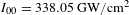
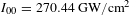
To determine the NLA properties of the sample, the Z-scan experiments were performed at different laser intensities (
 $I_{00}$
) adjusted by rotating the neutral density filter. Note that
$I_{00}$
) adjusted by rotating the neutral density filter. Note that
 $I_{00}$
is the on-axis peak intensity at the focus point. Since the band gap value of DKDP crystals is close to 7.8 eV[Reference Carr, Radousky and Demos12], four photons would be required to make an electron transition from the valence band (VB) to the CB. The four-photon absorption (4PA) theory[Reference Gu, Huang, Tan, Wang and Ji22] was used to fit the Z-scan results, where the value of linear absorption coefficient was calculated from the linear transmittance measured by a spectrophotometer (PE Lambda 1050) and evaluated to be
$I_{00}$
is the on-axis peak intensity at the focus point. Since the band gap value of DKDP crystals is close to 7.8 eV[Reference Carr, Radousky and Demos12], four photons would be required to make an electron transition from the valence band (VB) to the CB. The four-photon absorption (4PA) theory[Reference Gu, Huang, Tan, Wang and Ji22] was used to fit the Z-scan results, where the value of linear absorption coefficient was calculated from the linear transmittance measured by a spectrophotometer (PE Lambda 1050) and evaluated to be
 $0.196~\text{cm}^{-1}$
. As shown in Figure 1, the NLA phenomenon was observed at
$0.196~\text{cm}^{-1}$
. As shown in Figure 1, the NLA phenomenon was observed at
 $I_{00}=338.05~\text{GW}/\text{cm}^{2}$
, but not observed at
$I_{00}=338.05~\text{GW}/\text{cm}^{2}$
, but not observed at
 $I_{00}=270.44~\text{GW}/\text{cm}^{2}$
, and the NLA coefficient remained nearly constant. Therefore, the critical intensity for exciting the NLA (denoted as
$I_{00}=270.44~\text{GW}/\text{cm}^{2}$
, and the NLA coefficient remained nearly constant. Therefore, the critical intensity for exciting the NLA (denoted as
 $I_{\text{c}}$
) was between
$I_{\text{c}}$
) was between
 $I_{00}=270.44~\text{GW}/\text{cm}^{2}$
and
$I_{00}=270.44~\text{GW}/\text{cm}^{2}$
and
 $I_{00}=338.05~\text{GW}/\text{cm}^{2}$
. Here we roughly took
$I_{00}=338.05~\text{GW}/\text{cm}^{2}$
. Here we roughly took
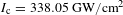 $I_{\text{c}}=338.05~\text{GW}/\text{cm}^{2}$
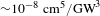
. The 4PA coefficient
$I_{\text{c}}=338.05~\text{GW}/\text{cm}^{2}$
. The 4PA coefficient
 $\unicode[STIX]{x1D6FC}_{4}$
was of the order of
$\unicode[STIX]{x1D6FC}_{4}$
was of the order of
 ${\sim}10^{-8}~\text{cm}^{5}/\text{GW}^{3}$
, and the corresponding 4PA cross section
${\sim}10^{-8}~\text{cm}^{5}/\text{GW}^{3}$
, and the corresponding 4PA cross section
 $\unicode[STIX]{x1D70E}_{\text{4PA}}$
was determined to be
$\unicode[STIX]{x1D70E}_{\text{4PA}}$
was determined to be
 ${\sim}10^{-110}~\text{cm}^{8}\cdot \text{s}^{3}$
by
${\sim}10^{-110}~\text{cm}^{8}\cdot \text{s}^{3}$
by
 $\unicode[STIX]{x1D70E}_{\text{4PA}}=(\hslash \unicode[STIX]{x1D714})^{3}\unicode[STIX]{x1D6FC}_{4}/N_{0}$
, where
$\unicode[STIX]{x1D70E}_{\text{4PA}}=(\hslash \unicode[STIX]{x1D714})^{3}\unicode[STIX]{x1D6FC}_{4}/N_{0}$
, where
 $N_{0}=5\times 10^{19}~\text{cm}^{-3}$
is the initial defect density[Reference Demos, DeMange, Negres and Feit13]. This value is four orders of magnitude larger than the representative value in wide band gap ideal materials, which is of the order of
$N_{0}=5\times 10^{19}~\text{cm}^{-3}$
is the initial defect density[Reference Demos, DeMange, Negres and Feit13]. This value is four orders of magnitude larger than the representative value in wide band gap ideal materials, which is of the order of
 $10^{-114}~\text{cm}^{8}\cdot \text{s}^{3}$
[Reference Carr, Radousky and Demos12, Reference Jones, Braunlich, Casper, Shen and Kelly23]. This indicates that the NLA process is not a pure 4PA process; a defect-state-assisted 4PA process may be present.
$10^{-114}~\text{cm}^{8}\cdot \text{s}^{3}$
[Reference Carr, Radousky and Demos12, Reference Jones, Braunlich, Casper, Shen and Kelly23]. This indicates that the NLA process is not a pure 4PA process; a defect-state-assisted 4PA process may be present.
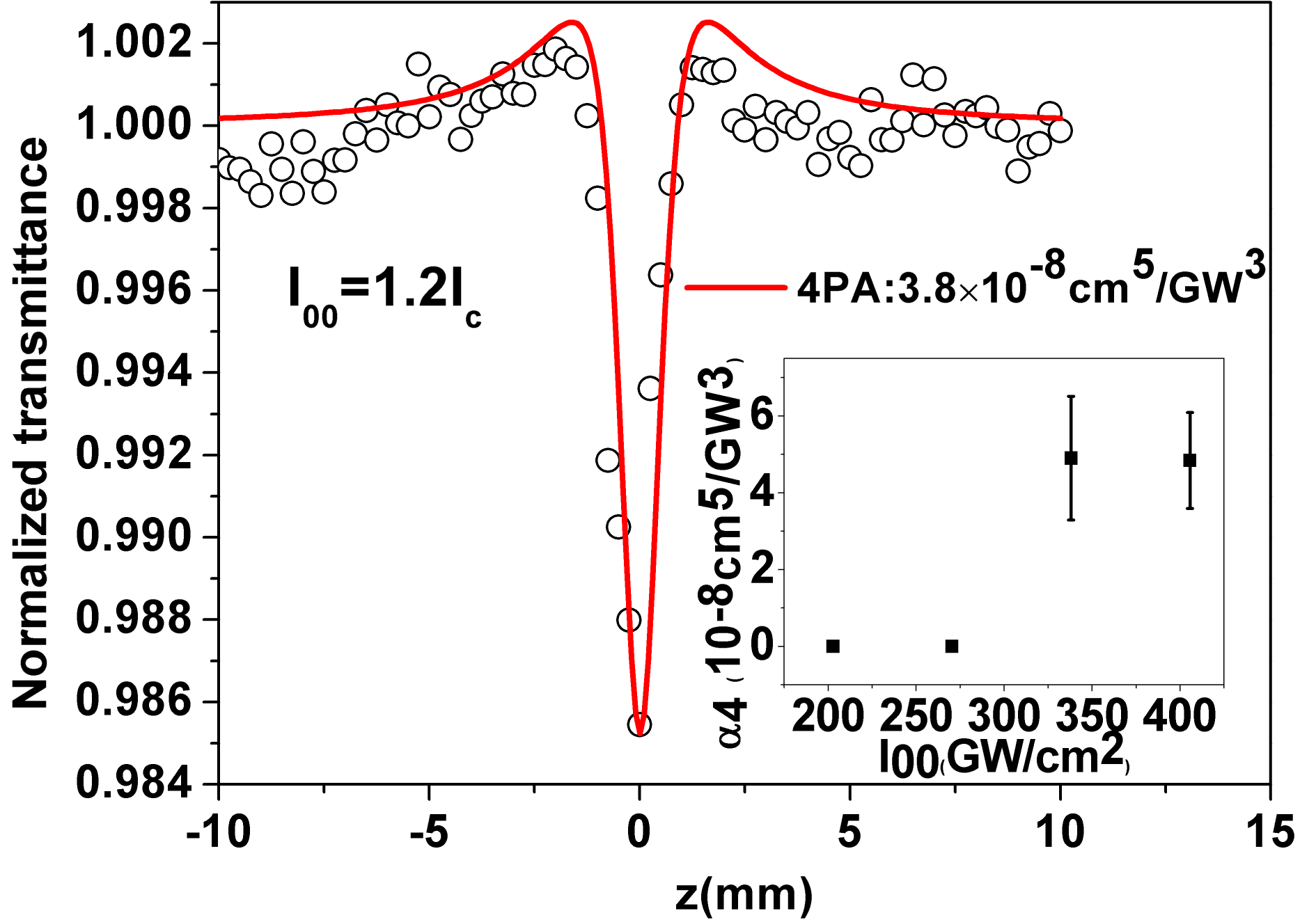
Figure 1. Representative OA Z-scan trace for the DKDP crystal at an excitation intensity of
 $1.2I_{\text{c}}$
. The circular symbols represent the experimental data, while the solid line is the theoretical fitting result by the use of the 4PA theory. The inset is the 4PA coefficient of the DKDP crystal at different excitation laser intensities, while the error bars are the standard deviation from five Z-scan experiments.
$1.2I_{\text{c}}$
. The circular symbols represent the experimental data, while the solid line is the theoretical fitting result by the use of the 4PA theory. The inset is the 4PA coefficient of the DKDP crystal at different excitation laser intensities, while the error bars are the standard deviation from five Z-scan experiments.
The OA Z-scan trace displays a symmetric valley with respect to the focus, as shown in Figure 1. However, at an excitation intensity
 $I_{00}=1.4I_{\text{c}}$
(denoted as
$I_{00}=1.4I_{\text{c}}$
(denoted as
 $I_{\text{tc}}$
), the symmetric valley changes, as shown in Figure 2. The Z-scan trace can be divided into three parts: (i) the transmittance first drops slowly along the Z direction; (ii) then the transmittance experiences a sharp drop near the focus point; (iii) the transmittance then rises slowly away from the focus point. The numerical simulation using the 4PA theory cannot fit the whole dataset well. It seems that there is a change of multiphoton absorption mechanism during this process. The (
$I_{\text{tc}}$
), the symmetric valley changes, as shown in Figure 2. The Z-scan trace can be divided into three parts: (i) the transmittance first drops slowly along the Z direction; (ii) then the transmittance experiences a sharp drop near the focus point; (iii) the transmittance then rises slowly away from the focus point. The numerical simulation using the 4PA theory cannot fit the whole dataset well. It seems that there is a change of multiphoton absorption mechanism during this process. The (
 $1+3$
) PA theory and (
$1+3$
) PA theory and (
 $1+2+1$
) PA theory mentioned below can fit well with the left and right data, respectively.
$1+2+1$
) PA theory mentioned below can fit well with the left and right data, respectively.
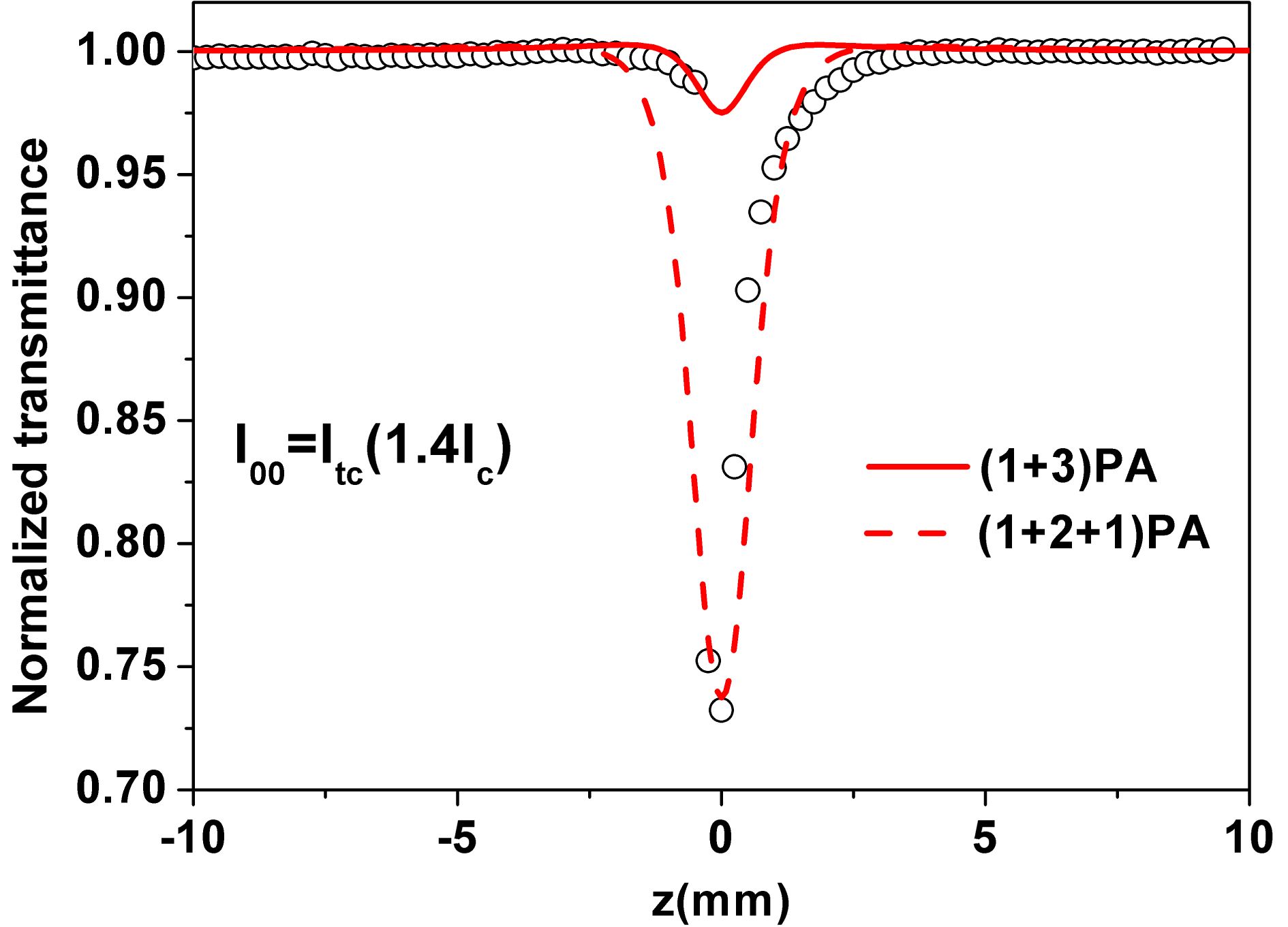
Figure 2. Representative OA Z-scan trace for the DKDP crystal at the excitation intensity of
 $I_{00}=I_{\text{tc}}$
. The circular symbols are the experimental data, while the solid (dotted) line is the theoretical fitting result by the use of the (
$I_{00}=I_{\text{tc}}$
. The circular symbols are the experimental data, while the solid (dotted) line is the theoretical fitting result by the use of the (
 $1+3$
) PA theory ((
$1+3$
) PA theory ((
 $1+2+1$
) PA theory).
$1+2+1$
) PA theory).
Moreover, as shown in Figure 3, after the site is excited with intensity
 $I_{\text{tc}}$
, the phenomenon of NLA becomes more pronounced, and the change lingers for a long time. Furthermore, the phenomenon of NLA can be observed at excitation intensities below
$I_{\text{tc}}$
, the phenomenon of NLA becomes more pronounced, and the change lingers for a long time. Furthermore, the phenomenon of NLA can be observed at excitation intensities below
 $I_{\text{c}}$
after the site is excited with intensity
$I_{\text{c}}$
after the site is excited with intensity
 $I_{\text{tc}}$
.
$I_{\text{tc}}$
.
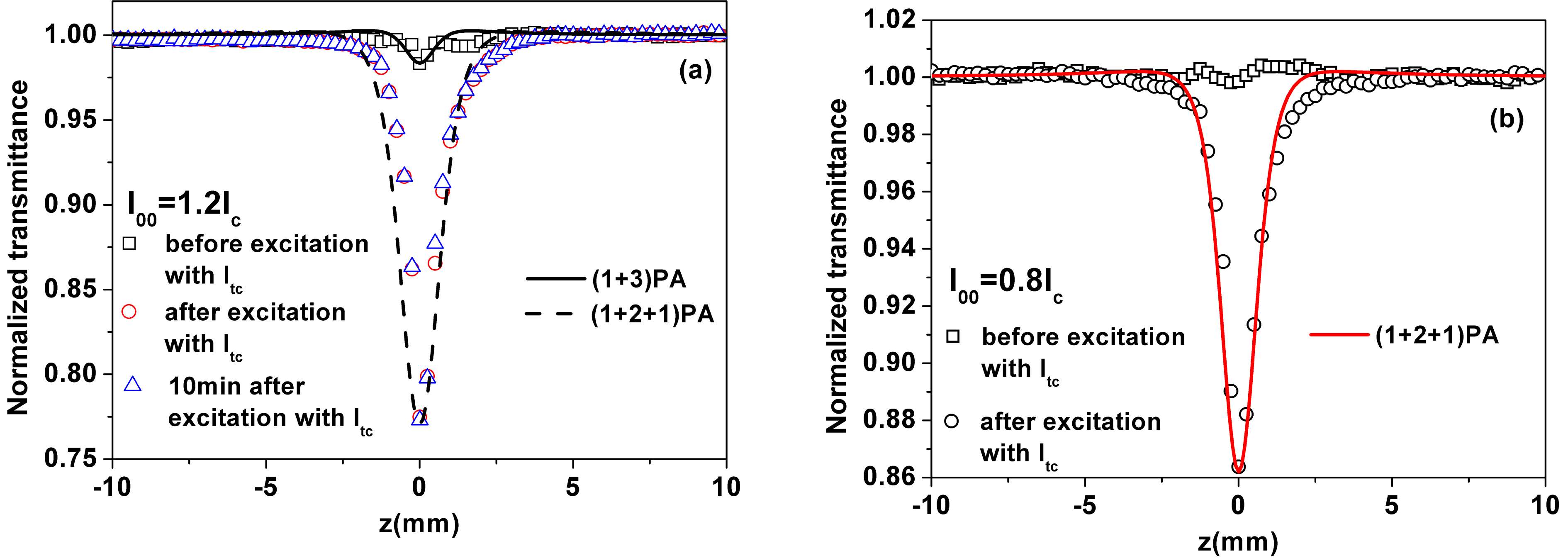
Figure 3. (a) The OA Z-scan traces for the DKDP crystal at the excitation intensity of
 $I_{00}=1.2I_{\text{c}}$
. Squares, circles and triangles are the experimental data before excitation with
$I_{00}=1.2I_{\text{c}}$
. Squares, circles and triangles are the experimental data before excitation with
 $I_{\text{tc}}$
, after excitation with
$I_{\text{tc}}$
, after excitation with
 $I_{\text{tc}}$
and about 10 min after excitation with
$I_{\text{tc}}$
and about 10 min after excitation with
 $I_{\text{tc}}$
, respectively. The solid (dotted) line is the theoretical fitting result using the (
$I_{\text{tc}}$
, respectively. The solid (dotted) line is the theoretical fitting result using the (
 $1+3$
) PA theory ((
$1+3$
) PA theory ((
 $1+2+1$
) PA theory). (b) The OA Z-scan traces for the DKDP crystal at
$1+2+1$
) PA theory). (b) The OA Z-scan traces for the DKDP crystal at
 $I_{00}=0.8I_{\text{c}}$
. Squares and circles are the experimental data before excitation with
$I_{00}=0.8I_{\text{c}}$
. Squares and circles are the experimental data before excitation with
 $I_{\text{tc}}$
and after excitation with
$I_{\text{tc}}$
and after excitation with
 $I_{\text{tc}}$
, respectively. The solid line is the theoretical fitting result obtained using the (
$I_{\text{tc}}$
, respectively. The solid line is the theoretical fitting result obtained using the (
 $1+2+1$
) PA theory.
$1+2+1$
) PA theory.
The previous results allow for the formation of a hypothesis about the NLA properties of the DKDP crystal at different laser intensities. The cluster of point defects introduces defect states in the band gap, which reduces the multiphoton order required to promote valance electrons to the CB. For a fresh site, the NLA process occurs only when the excitation intensity exceeds
 $I_{\text{c}}$
, and this process is a defect-state-assisted multiphoton absorption process, in which the electrons transfer into the CB through intraband states. When the site is excited with a higher intensity (larger than
$I_{\text{c}}$
, and this process is a defect-state-assisted multiphoton absorption process, in which the electrons transfer into the CB through intraband states. When the site is excited with a higher intensity (larger than
 $I_{\text{tc}}$
), before the focus point, the defect-state-assisted multiphoton absorption process occurs in a similar manner to when the sites were excited by
$I_{\text{tc}}$
), before the focus point, the defect-state-assisted multiphoton absorption process occurs in a similar manner to when the sites were excited by
 $I_{00}<I_{\text{tc}}$
. Near the focus point, the laser intensity is very strong and produces new defect states in the band gap. The new defect states further reduce the order of the multiphoton absorption needed for the electron transition. Therefore, the NLA after the focus point is improved. Since this process is not recoverable, the new defect states make the NLA process easier to excite and be observed at excitation intensities below
$I_{00}<I_{\text{tc}}$
. Near the focus point, the laser intensity is very strong and produces new defect states in the band gap. The new defect states further reduce the order of the multiphoton absorption needed for the electron transition. Therefore, the NLA after the focus point is improved. Since this process is not recoverable, the new defect states make the NLA process easier to excite and be observed at excitation intensities below
 $I_{\text{c}}$
. The observed
$I_{\text{c}}$
. The observed
 $I_{\text{tc}}$
can be understood as the critical intensity of the multiphoton absorption mechanism transition.
$I_{\text{tc}}$
can be understood as the critical intensity of the multiphoton absorption mechanism transition.
To confirm the above-mentioned analysis and further interpret the experimental data, we propose a model based on the change of multiphoton absorption mechanism induced by the transformation of defect species. We assume that the DKDP crystal undergoes a (
 $1+3$
) PA process before excitation with intensity
$1+3$
) PA process before excitation with intensity
 $I_{\text{tc}}$
. Since electronic structure models with two defect states in the band gap proposed by Demos et al. and Duchateau et al. can interpret some experimental results well[Reference Demos, DeMange, Negres and Feit13, Reference Duchateau, Geoffroy, Dyan, Piombini and Guizard14], we combine their analysis of the possible location of the defect states, and consider that a new defect state located in the band gap is produced after excitation with intensity
$I_{\text{tc}}$
. Since electronic structure models with two defect states in the band gap proposed by Demos et al. and Duchateau et al. can interpret some experimental results well[Reference Demos, DeMange, Negres and Feit13, Reference Duchateau, Geoffroy, Dyan, Piombini and Guizard14], we combine their analysis of the possible location of the defect states, and consider that a new defect state located in the band gap is produced after excitation with intensity
 $I_{\text{tc}}$
followed by the (
$I_{\text{tc}}$
followed by the (
 $1+2+1$
) PA process, as shown in Figure 4. A possible example of the transformation of defect species is an oxygen vacancy. After excitation with intensity
$1+2+1$
) PA process, as shown in Figure 4. A possible example of the transformation of defect species is an oxygen vacancy. After excitation with intensity
 $I_{\text{tc}}$
, a large number of electrons and holes are produced. Some of the holes can be trapped at neutral O vacancies and lead to the production of
$I_{\text{tc}}$
, a large number of electrons and holes are produced. Some of the holes can be trapped at neutral O vacancies and lead to the production of
 $+1$
charged O vacancies[Reference Evans, Giles, Halliburton and Kappers24]. The defect is transformed from a neutral O vacancy, which provides only one state in the band gap, into a
$+1$
charged O vacancies[Reference Evans, Giles, Halliburton and Kappers24]. The defect is transformed from a neutral O vacancy, which provides only one state in the band gap, into a
 $+1$
charged O vacancy, which can provide two states[Reference Liu, Hou, Kioussis, Demos and Radousky11].
$+1$
charged O vacancy, which can provide two states[Reference Liu, Hou, Kioussis, Demos and Radousky11].
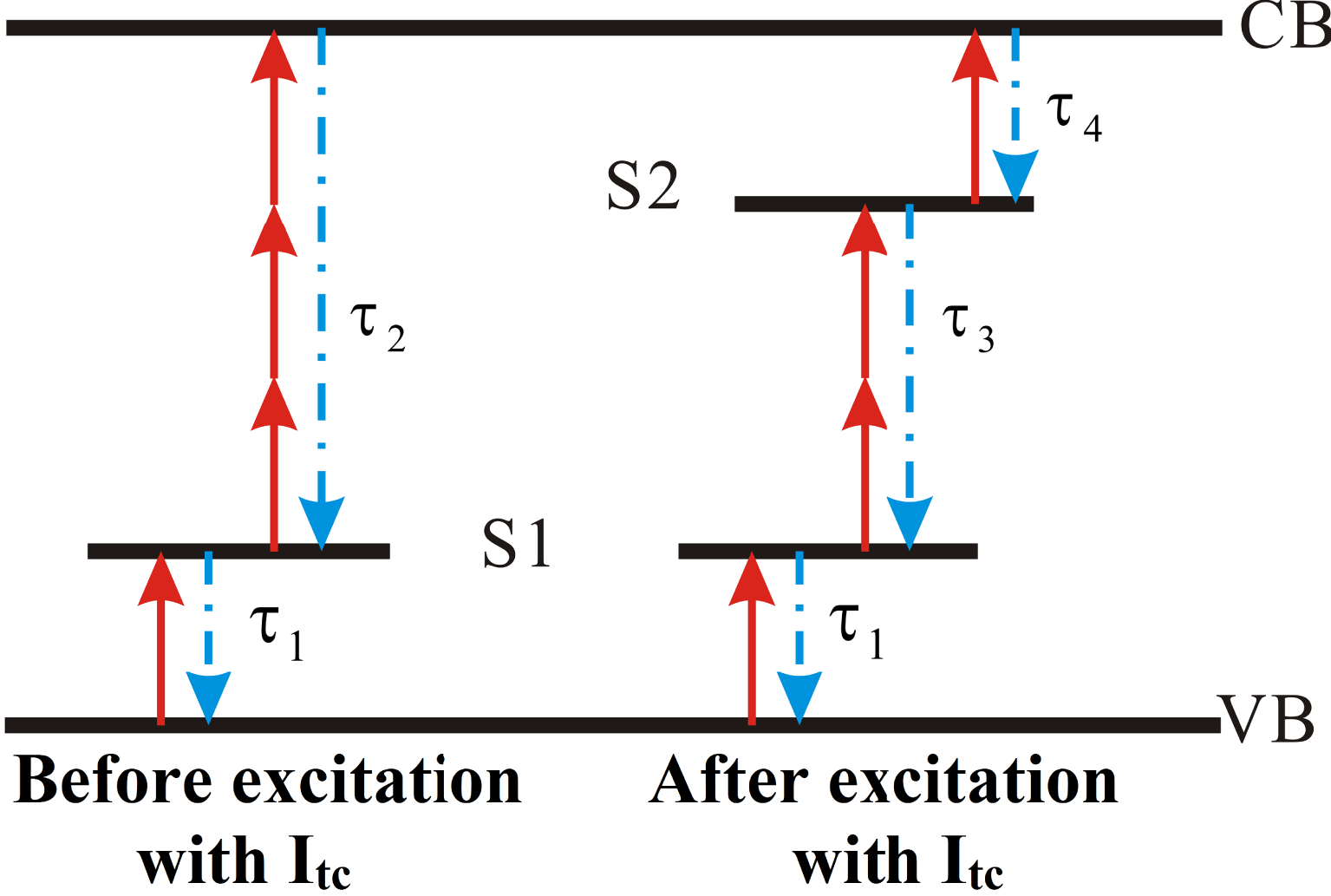
Figure 4. Schematic illustration of the band structure. The solid arrows indicate the absorption of photons, whereas the dash-dotted arrows indicate the relaxation process. S1 and S2 are the states located in the band gap.
The attenuation of the pulse intensity as light propagates through the sample can be described as follows.
Before excitation with intensity
 $I_{\text{tc}}$
:
$I_{\text{tc}}$
:
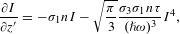
 $$\begin{eqnarray}\displaystyle \frac{\unicode[STIX]{x2202}I}{\unicode[STIX]{x2202}z^{\prime }}=-\unicode[STIX]{x1D70E}_{1}In_{0}-\frac{\unicode[STIX]{x1D70E}_{3}}{(\hslash \unicode[STIX]{x1D714})^{2}}I^{3}n_{1}. & & \displaystyle\end{eqnarray}$$
After excitation with intensity
 $I_{\text{tc}}$
:
$I_{\text{tc}}$
:
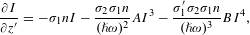
 $$\begin{eqnarray}\displaystyle \frac{\unicode[STIX]{x2202}I}{\unicode[STIX]{x2202}z^{\prime }}=-\unicode[STIX]{x1D70E}_{1}In_{0}-\frac{\unicode[STIX]{x1D70E}_{2}}{\hslash \unicode[STIX]{x1D714}}I^{2}n_{1}-\unicode[STIX]{x1D70E}_{1}^{\prime }In_{2}, & & \displaystyle\end{eqnarray}$$
where
 $z^{\prime }$
is the propagation length inside the sample;
$z^{\prime }$
is the propagation length inside the sample;
 $\unicode[STIX]{x1D70E}_{1}$
is the one-photon absorption (1PA) cross section to bridge the VB to S1,
$\unicode[STIX]{x1D70E}_{1}$
is the one-photon absorption (1PA) cross section to bridge the VB to S1,
 $\unicode[STIX]{x1D70E}_{1}^{\prime }$
is the 1PA cross section to bridge S2 to the CB,
$\unicode[STIX]{x1D70E}_{1}^{\prime }$
is the 1PA cross section to bridge S2 to the CB,
 $\unicode[STIX]{x1D70E}_{2}$
is the two-photon absorption (2PA) cross section to bridge S1 to S2 and
$\unicode[STIX]{x1D70E}_{2}$
is the two-photon absorption (2PA) cross section to bridge S1 to S2 and
 $\unicode[STIX]{x1D70E}_{3}$
is the three-photon absorption (3PA) cross section to bridge S1 to the CB;
$\unicode[STIX]{x1D70E}_{3}$
is the three-photon absorption (3PA) cross section to bridge S1 to the CB;
 $n_{0}$
,
$n_{0}$
,
 $n_{1}$
and
$n_{1}$
and
 $n_{2}$
are the electron densities in the VB, S1 and S2, respectively.
$n_{2}$
are the electron densities in the VB, S1 and S2, respectively.
The populations of states can be described by a simple set of rate equations as follows.
Before excitation with intensity
 $I_{\text{tc}}$
:
$I_{\text{tc}}$
:
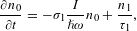 $$\begin{eqnarray}\displaystyle & \displaystyle \frac{\unicode[STIX]{x2202}n_{0}}{\unicode[STIX]{x2202}t}=-\unicode[STIX]{x1D70E}_{1}\frac{I}{\hslash \unicode[STIX]{x1D714}}n_{0}+\frac{n_{1}}{\unicode[STIX]{x1D70F}_{1}}, & \displaystyle\end{eqnarray}$$
 $$\begin{eqnarray}\displaystyle & \displaystyle \frac{\unicode[STIX]{x2202}n_{1}}{\unicode[STIX]{x2202}t}=\unicode[STIX]{x1D70E}_{1}\frac{I}{\hslash \unicode[STIX]{x1D714}}n_{0}-\unicode[STIX]{x1D70E}_{3}\left(\frac{I}{\hslash \unicode[STIX]{x1D714}}\right)^{3}n_{1}+\frac{n_{cb}}{\unicode[STIX]{x1D70F}_{2}}-\frac{n_{1}}{\unicode[STIX]{x1D70F}_{1}}, & \displaystyle\end{eqnarray}$$
 $$\begin{eqnarray}\displaystyle & \displaystyle \frac{\unicode[STIX]{x2202}n_{cb}}{\unicode[STIX]{x2202}t}=\unicode[STIX]{x1D70E}_{3}\left(\frac{I}{\hslash \unicode[STIX]{x1D714}}\right)^{3}n_{1}-\frac{n_{cb}}{\unicode[STIX]{x1D70F}_{2}}, & \displaystyle\end{eqnarray}$$
 $$\begin{eqnarray}\displaystyle & \displaystyle n=n_{0}+n_{1}+n_{cb}. & \displaystyle\end{eqnarray}$$
 $I_{\text{tc}}$
:
$I_{\text{tc}}$
:  $$\begin{eqnarray}\displaystyle & \displaystyle \frac{\unicode[STIX]{x2202}n_{0}}{\unicode[STIX]{x2202}t}=-\unicode[STIX]{x1D70E}_{1}\frac{I}{\hslash \unicode[STIX]{x1D714}}n_{0}+\frac{n_{1}}{\unicode[STIX]{x1D70F}_{1}}, & \displaystyle\end{eqnarray}$$
 $$\begin{eqnarray}\displaystyle & \displaystyle \frac{\unicode[STIX]{x2202}n_{1}}{\unicode[STIX]{x2202}t}=\unicode[STIX]{x1D70E}_{1}\frac{I}{\hslash \unicode[STIX]{x1D714}}n_{0}-\unicode[STIX]{x1D70E}_{2}\left(\frac{I}{\hslash \unicode[STIX]{x1D714}}\right)^{2}n_{1}+\frac{n_{2}}{\unicode[STIX]{x1D70F}_{3}}-\frac{n_{1}}{\unicode[STIX]{x1D70F}_{1}}, & \displaystyle\end{eqnarray}$$
 $$\begin{eqnarray}\displaystyle & \displaystyle \frac{\unicode[STIX]{x2202}n_{2}}{\unicode[STIX]{x2202}t}=\unicode[STIX]{x1D70E}_{2}\left(\frac{I}{\hslash \unicode[STIX]{x1D714}}\right)^{2}n_{1}-\unicode[STIX]{x1D70E}_{1}^{\prime }\frac{I}{\hslash \unicode[STIX]{x1D714}}n_{2}+\frac{n_{cb}}{\unicode[STIX]{x1D70F}_{4}}-\frac{n_{2}}{\unicode[STIX]{x1D70F}_{3}}, & \displaystyle\end{eqnarray}$$
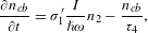 $$\begin{eqnarray}\displaystyle & \displaystyle \frac{\unicode[STIX]{x2202}n_{cb}}{\unicode[STIX]{x2202}t}=\unicode[STIX]{x1D70E}_{1}^{\prime }\frac{I}{\hslash \unicode[STIX]{x1D714}}n_{2}-\frac{n_{cb}}{\unicode[STIX]{x1D70F}_{4}}, & \displaystyle\end{eqnarray}$$
 $$\begin{eqnarray}\displaystyle & \displaystyle n=n_{0}+n_{1}+n_{2}+n_{cb}, & \displaystyle\end{eqnarray}$$
 $\unicode[STIX]{x1D70F}_{1}$
,
$\unicode[STIX]{x1D70F}_{1}$
,
 $\unicode[STIX]{x1D70F}_{2}$
,
$\unicode[STIX]{x1D70F}_{2}$
,
 $\unicode[STIX]{x1D70F}_{3}$
and
$\unicode[STIX]{x1D70F}_{3}$
and
 $\unicode[STIX]{x1D70F}_{4}$
are the relaxation times of S1 to the VB, the CB to S1, S2 to S1 and the CB to S2, respectively;
$\unicode[STIX]{x1D70F}_{4}$
are the relaxation times of S1 to the VB, the CB to S1, S2 to S1 and the CB to S2, respectively;
 $n$
and
$n$
and
 $n_{cb}$
are the initial electron density in the VB and electron density in the CB, respectively. The value of
$n_{cb}$
are the initial electron density in the VB and electron density in the CB, respectively. The value of
 $n_{cb}$
is close to zero at relatively low energy excitation conditions since the electrons pumped onto the CB jump back promptly due to the short relaxation time from the CB to the defect state. In this analysis, we emphasize that the transition only takes place in the vicinity of the defects and assume that the VB is not sufficiently depleted for the light excitations used in the model. Therefore
$n_{cb}$
is close to zero at relatively low energy excitation conditions since the electrons pumped onto the CB jump back promptly due to the short relaxation time from the CB to the defect state. In this analysis, we emphasize that the transition only takes place in the vicinity of the defects and assume that the VB is not sufficiently depleted for the light excitations used in the model. Therefore
 $n_{1}\ll n$
,
$n_{1}\ll n$
,
 $n_{2}\ll n$
; we set
$n_{2}\ll n$
; we set
 $n_{0}\approx n=N_{0}$
. Under the excitation of the ultrafast laser with a spatial and temporal Gaussian profile, we have
$n_{0}\approx n=N_{0}$
. Under the excitation of the ultrafast laser with a spatial and temporal Gaussian profile, we have
 $I=I_{0}\exp (-t^{2}/\unicode[STIX]{x1D70F}^{2})$
, where
$I=I_{0}\exp (-t^{2}/\unicode[STIX]{x1D70F}^{2})$
, where
 $I_{0}$
gives the spatial profile and
$I_{0}$
gives the spatial profile and
 $\unicode[STIX]{x1D70F}$
is the pulse width. Considering that
$\unicode[STIX]{x1D70F}$
is the pulse width. Considering that
 $\unicode[STIX]{x1D70F}_{1}$
is of the order of 1 ns or shorter and
$\unicode[STIX]{x1D70F}_{1}$
is of the order of 1 ns or shorter and
 $\unicode[STIX]{x1D70F}_{3}$
is of the picosecond time scale (
$\unicode[STIX]{x1D70F}_{3}$
is of the picosecond time scale (
 $\unicode[STIX]{x1D70F}$
is much smaller than the relaxation times)[Reference Demos, DeMange, Negres and Feit13], the population densities of S1 and S2 are as follows.
$\unicode[STIX]{x1D70F}$
is much smaller than the relaxation times)[Reference Demos, DeMange, Negres and Feit13], the population densities of S1 and S2 are as follows. Before excitation with intensity
 $I_{\text{tc}}$
:
$I_{\text{tc}}$
:
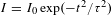
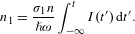 $$\begin{eqnarray}\displaystyle n_{1}=\frac{\unicode[STIX]{x1D70E}_{1}n}{\hslash \unicode[STIX]{x1D714}}\int _{-\infty }^{t}I(t^{\prime })\,\text{d}t^{\prime }. & & \displaystyle\end{eqnarray}$$
After excitation with intensity
 $I_{\text{tc}}$
:
$I_{\text{tc}}$
:
 $$\begin{eqnarray}\displaystyle & \displaystyle n_{1}=\frac{\unicode[STIX]{x1D70E}_{1}n}{\hslash \unicode[STIX]{x1D714}}\int _{-\infty }^{t}\!\!I(t^{\prime })\exp \left\{\unicode[STIX]{x1D70E}_{2}\left(\frac{I_{0}}{\hslash \unicode[STIX]{x1D714}}\right)^{2}\frac{\sqrt{2\unicode[STIX]{x1D70B}}\unicode[STIX]{x1D70F}}{4}\left[\text{erf}\!\left(\frac{\sqrt{2}t^{\prime }}{\unicode[STIX]{x1D70F}}\right)\right.\right. & \displaystyle \nonumber\\ \displaystyle & \displaystyle \hspace{-102.0pt}\left.\left.-\,\text{erf}\left(\frac{\sqrt{2}t}{\unicode[STIX]{x1D70F}}\right)\right]\right\}\,\text{d}t^{\prime }, & \displaystyle\end{eqnarray}$$
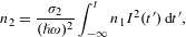 $$\begin{eqnarray}\displaystyle & \displaystyle n_{2}=\frac{\unicode[STIX]{x1D70E}_{2}}{(\hslash \unicode[STIX]{x1D714})^{2}}\int _{-\infty }^{t}n_{1}I^{2}(t^{\prime })\,\text{d}t^{\prime }, & \displaystyle\end{eqnarray}$$
 $\text{erf}(x)$
is the error function.
$\text{erf}(x)$
is the error function.
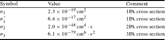
Table 1. Value of the parameters used in the fitting.
We could revise Equations (1) and (2) with the space and time average approximation method[Reference Sutherland25, Reference Gu and Ji26] as
 $$\begin{eqnarray}\displaystyle & \displaystyle \frac{\unicode[STIX]{x2202}I}{\unicode[STIX]{x2202}z^{\prime }}=-\unicode[STIX]{x1D70E}_{1}nI-\sqrt{\frac{\unicode[STIX]{x1D70B}}{3}}\frac{\unicode[STIX]{x1D70E}_{3}\unicode[STIX]{x1D70E}_{1}n\unicode[STIX]{x1D70F}}{(\hslash \unicode[STIX]{x1D714})^{3}}I^{4}, & \displaystyle\end{eqnarray}$$
 $$\begin{eqnarray}\displaystyle & \displaystyle \frac{\unicode[STIX]{x2202}I}{\unicode[STIX]{x2202}z^{\prime }}=-\unicode[STIX]{x1D70E}_{1}nI-\frac{\unicode[STIX]{x1D70E}_{2}\unicode[STIX]{x1D70E}_{1}n}{(\hslash \unicode[STIX]{x1D714})^{2}}AI^{3}-\frac{\unicode[STIX]{x1D70E}_{1}^{\prime }\unicode[STIX]{x1D70E}_{2}\unicode[STIX]{x1D70E}_{1}n}{(\hslash \unicode[STIX]{x1D714})^{3}}BI^{4}, & \displaystyle\end{eqnarray}$$
where
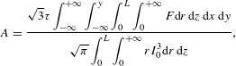 $$\begin{eqnarray}\displaystyle & \displaystyle A=\frac{\sqrt{3}\unicode[STIX]{x1D70F}\displaystyle \int _{-\infty }^{+\infty }\int _{-\infty }^{y}\int _{0}^{L}\int _{0}^{+\infty }F\text{d}r\,\text{d}z\,\text{d}x\,\text{d}y}{\sqrt{\unicode[STIX]{x1D70B}}\displaystyle \int _{0}^{L}\int _{0}^{+\infty }rI_{0}^{3}\text{d}r\,\text{d}z}, & \displaystyle\end{eqnarray}$$
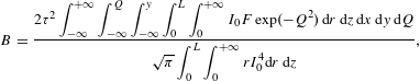 $$\begin{eqnarray}\displaystyle & \displaystyle B=\frac{2\unicode[STIX]{x1D70F}^{2}\displaystyle \int _{-\infty }^{+\infty }\int _{-\infty }^{Q}\int _{-\infty }^{y}\int _{0}^{L}\int _{0}^{+\infty }I_{0}F\exp (-Q^{2})\,\text{d}r\,\text{d}z\,\text{d}x\,\text{d}y\,\text{d}Q}{\sqrt{\unicode[STIX]{x1D70B}}\displaystyle \int _{0}^{L}\int _{0}^{+\infty }rI_{0}^{4}\text{d}r\,\text{d}z}, & \displaystyle \nonumber\\ \displaystyle & & \displaystyle\end{eqnarray}$$
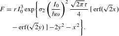 $$\begin{eqnarray}\displaystyle & \displaystyle F=rI_{0}^{3}\exp \biggl\{\unicode[STIX]{x1D70E}_{2}\left(\frac{I_{0}}{\hslash \unicode[STIX]{x1D714}}\right)^{2}\frac{\sqrt{2\unicode[STIX]{x1D70B}}\unicode[STIX]{x1D70F}}{4} [\text{erf}(\sqrt{2}x) & \displaystyle \nonumber\\ \displaystyle & \displaystyle \hspace{-30.0pt}-\,\text{erf}(\sqrt{2}y)]-2y^{2}-x^{2}\biggr\}. & \displaystyle\end{eqnarray}$$
Equation (7) is formally consistent with the light propagation equation which describes the 4PA process in the sample. Equation (8) is formally consistent with the light propagation equation which describes the concurrence of 3PA process and 4PA process in the sample. Therefore, we can use the results from Ref. [Reference Gu, Huang, Tan, Wang and Ji22] to fit our experimental data. As can be seen in Figures 2 and 3, the fit lines are in good agreement with the experimental data. For the entire range of intensities, the best fit of the experimental data is obtained with the parameter values summarized in Table 1. The obtained generalized multiphoton absorption cross sections are comparable to the empirical formula[Reference Agostini and Petite27].
4 Conclusions
In summary, based on the Z-scan technique, the NLA properties of the DKDP crystal at 515 nm under different excitation laser intensities were investigated. This study has shown that two critical intensities exist: (i) the critical intensity (
 $I_{\text{c}}$
) for exciting the NLA (as the intensity exceeds
$I_{\text{c}}$
) for exciting the NLA (as the intensity exceeds
 $I_{\text{c}}$
, 4PA is observed and the absorption cross section is larger than the representative value in wide band gap ideal materials); (ii) the critical intensity (
$I_{\text{c}}$
, 4PA is observed and the absorption cross section is larger than the representative value in wide band gap ideal materials); (ii) the critical intensity (
 $I_{\text{tc}}$
) of the multiphoton absorption mechanism transition (after the site is excited with an intensity larger than
$I_{\text{tc}}$
) of the multiphoton absorption mechanism transition (after the site is excited with an intensity larger than
 $I_{\text{tc}}$
, the phenomenon of NLA is enhanced and can be observed below the
$I_{\text{tc}}$
, the phenomenon of NLA is enhanced and can be observed below the
 $I_{\text{c}}$
value). The experimental data are supported by a model based on the change of multiphoton absorption mechanism induced by the transformation of defect species, which can provide a different number of states in the band gap. These results clearly show the existence of defect states in the band gap, which can assist in multiphoton absorption and be manipulated by varying laser intensity.
$I_{\text{c}}$
value). The experimental data are supported by a model based on the change of multiphoton absorption mechanism induced by the transformation of defect species, which can provide a different number of states in the band gap. These results clearly show the existence of defect states in the band gap, which can assist in multiphoton absorption and be manipulated by varying laser intensity.
Acknowledgement
This work is supported by the National Natural Science Foundation of China (Nos. 61405219 and 11304328).


 Open access