


Introduction
X-ray microscopy is a powerful characterization tool applied in many scientific fields, such as materials science, environmental science, biology, and energy research [Reference Shapiro1–Reference Calvo-Almazán4]. With the advances in synchrotron source brilliance and efficient X-ray focusing optics, significant progress has been made in applying X-ray beams for nanoscale analysis. X-rays with high photon energies (typically above several keVs) are called hard X-rays, which have sufficient penetration depth and depth-of- focus for most nanoscale specimens, while providing excellent imaging resolution. However, imaging with hard X-rays faces challenges in both optics and microscopy systems. The most frequently used optics for X-ray nano focusing include Fresnel zone plates, Kirkpatrick-Baez (KB) mirrors, and multilayer Laue lenses (MLLs) [Reference Yan5–Reference Nazaretski7]. Among others, MLLs have been proposed and employed for high-efficiency nanofocusing in the hard X-ray regime [Reference Kang8–Reference Yan10]. MLLs are diffractive optics made of layers of alternating materials with different refractive indices (for example, WSi2/Si, W/SiC, and WC/SiC). Since MLLs are one-dimensional focusing elements, in order to achieve point focusing, two MLLs must be orthogonally aligned with one another [Reference Yan11] (Figure 1). This involves eight independent motions with nanoscale resolution. For instance, to maintain a 10 nm diffraction-limited point focus, the tolerance for orthogonal misalignment should be less than 0.01°, and the distance between the focal planes of two MLLs should be less than the depth of focus (for example, ~2 μm) [Reference Yan12]. Moreover, when nm-scale spatial resolution imaging is considered, the stability of the MLLs and their alignment also needs to be maintained. These requirements pose significant technical challenges for a microscopy system and require an extremely complex and stable instrument.
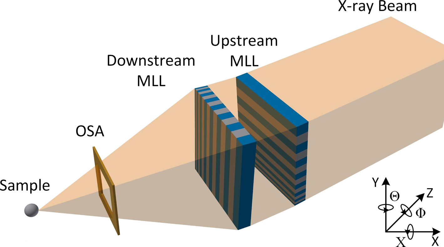
Figure 1: Schematic of MLL-based X-ray microscope. A total of eight degrees of rotational and translational motions are required to perform full alignment of two linear MLLs. A central beamstop is not shown in the schematic.
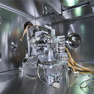
Several sophisticated MLL-based instruments have been designed, constructed, and commissioned in recent years [Reference Nazaretski13–Reference Nazaretski17]. For instance, a high-resolution scanning hard X-ray microscope has been developed at the Hard X-ray Nanoprobe (HXN) beamline of the National Synchrotron Light Source II (NSLS-II) (Figure 2). It utilizes two individual MLL nanofocusing optics to provide non-destructive chemical mapping with unprecedented spatial resolution approaching 10 nm in 2D and 3D [Reference Yan5,Reference Nazaretski17,Reference Michelson18]. The HXN end station utilizes state-of-the-art piezo-mechanical components and offers positioning accuracy of just a few nanometers. While it works well for many experiments, the alignment procedure of two individual MLLs in the current system is rather complex. Moreover, when performing focusing experiments below 10 nm, space constraints start to play a role, making alignment even more complex.
Figure 2: The MLL microscope module at Hard X-ray Nanoprobe (HXN) beamline of the National Synchrotron Light Source II (NSLS-II).
The development of monolithic pre-aligned 2D MLL nanofocusing optics could minimize degrees of the nanoscale motion needed for MLL alignment and substantially reduce the complexity of an instrument. Over the past few years, many initiatives have been made to develop monolithic 2D MLL optics [Reference Niese19–Reference Kubec22], such as UV-adhesive assisted direct bonding of MLL structures. However, uncontrollable stress and potential contamination from UV adhesives make the direct bonding approach very difficult.
In this article, we report our recently developed monolithic MEMS-based 2D MLL nanofocusing optics for high-resolution hard X-ray microscopy [Reference Xu23]. By utilizing microfabrication technologies, MEMS-based silicon templates to accommodate two linear MLL optics in a pre-aligned configuration, which significantly simplify the MLLs alignment process, were manufactured. Using the developed 2D MLL structure, an astigmatism-free point focus of ~14 nm by ~13 nm in horizontal and vertical directions, respectively, at 13.6 keV photon energy is demonstrated. The new system dramatically alleviates the design constraints and complexity of the MLL microscope. Furthermore, due to the reduced complexity, the new system is compatible with more conventional and widely used zoneplate-based X-ray microscopy systems, making high-resolution X-ray imaging more accessible at other synchrotron facilities.
Methods and Materials
Design of MEMS-based 2D MLL optics. A MEMS-based 2D MLL X-ray nano-focusing optics was designed by utilizing microfabrication techniques [Reference Xu23,Reference Xu24]. As shown in Figure 3, the entire optics consists of a MEMS template, two linear MLLs, and two adapters. The MEMS template, which is fabricated on an ~500 μm thick silicon wafer, has linear dimensions of ~10 × 10 × 0.5 mm3. On each side of the template, there is a microfabricated holding slot, which includes multiple alignment “teeth” and cantilever-typed silicon springs. Two holding slots on the front and back sides of the wafer are aligned orthogonally with a well-defined angle. There is an etched-through aperture at the center of the template. MLLs are accommodated in the holding slot, one on each side. Adapters are used if the sizes of MLLs do not fit into the holding slot. The mounted MLLs align to the alignment “teeth” and are pushed by the springs to secure their positions. The active optical regions of two MLL optics overlap at the aperture, where the X-ray beam passes through to illuminate both MLLs.
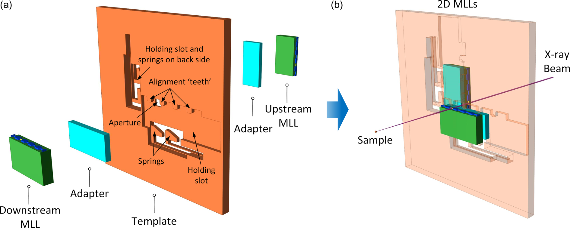
Figure 3: MEMS-based 2D MLL X-ray nanofocusing optics. (a) A MEMS template shows the key features, including holding slots, alignment “teeth,” springs, and an aperture. (b) 2D MLL optics assembled using the MEMS template. X-ray beam passes through the aperture, illuminates two overlapping MLLs, and focuses on the sample. Adapted with permission from [Reference Xu23] © The Optical Society.
The position of the MLLs mounted onto the template is precisely controlled by leveraging the high accuracy provided by microfabrication techniques. The angular position of the mounted MLLs is adjusted through the alignment teeth. By changing the length and distance of adjacent alignment teeth, the angle between two slots and, consequently, the orthogonality of MLLs mounted in the slots, can be changed. The separation distance between two lenses is adjusted by changing the depth of etched holding slots or the thickness of adapters so that it agrees with the focal length differences of two individual MLLs to achieve astigmatism-free point focus. For design details, please see [Reference Xu23,Reference Xu24].
Fabrication of MEMS-based templates. The MEMS templates were fabricated through a microfabrication process, which includes multiple steps of photolithography and deep reactive-ion etching (DRIE). The fabrication details are included in [Reference Xu23,Reference Xu24].
Fabrication of MLL optics. The MLL optics were fabricated via magnetron sputtering deposition on a silicon substrate and further sectioned by reactive ion etching, followed by focused ion beam (FIB) milling. The fabricated MLL optics were then characterized with respect to dimensions, morphology, and optical properties by optical microscopy, SEM, and interferometry.
Assembly of 2D MLL optics. Upon completion of the fabrication of MLL optics and MEMS templates, 1D lenses were mounted onto the template, and the 2D MLL optics were characterized with respect to orthogonality, separation distance, and stability. The orthogonality of the assembled 2D MLL was adjusted by changing templates. The separation distance of the assembled MLLs was characterized by using a white-light interferometer. The lateral position of two MLLs was adjusted under an optical microscope so their zone areas overlapped through the template aperture.
Results
MEMS template. Figure 4a shows an example of the microfabricated silicon template [Reference Xu23,Reference Xu24]. The overall lateral dimensions are ~10 × 10 mm2. On each side of the template, there is an etched holding slot, along with alignment teeth and springs. Two holding slots on the front and back sides are aligned orthogonally to each other. Figure 4a-ii shows an SEM image of the holding slot. The etching depth of slots depends on the used MLLs, typically between 150 and 250 μm. It can be modified by changing the number of etching cycles with submicron resolution. By changing the length difference of adjacent alignment teeth, a set of templates was fabricated with the angle between two slots gradually changed from 89.7° to 90.3° with an angular increment of ~25 millidegrees. By using a template with the most appropriate slot angle, the angular misalignment induced by the various factors was minimized. The template can directly accommodate most of the available MLLs, which have a height of ~1.5 mm. For MLLs that could not be directly mounted into the slot, an adapter was first bonded with the MLL, and then the entire piece was mounted into the slot.
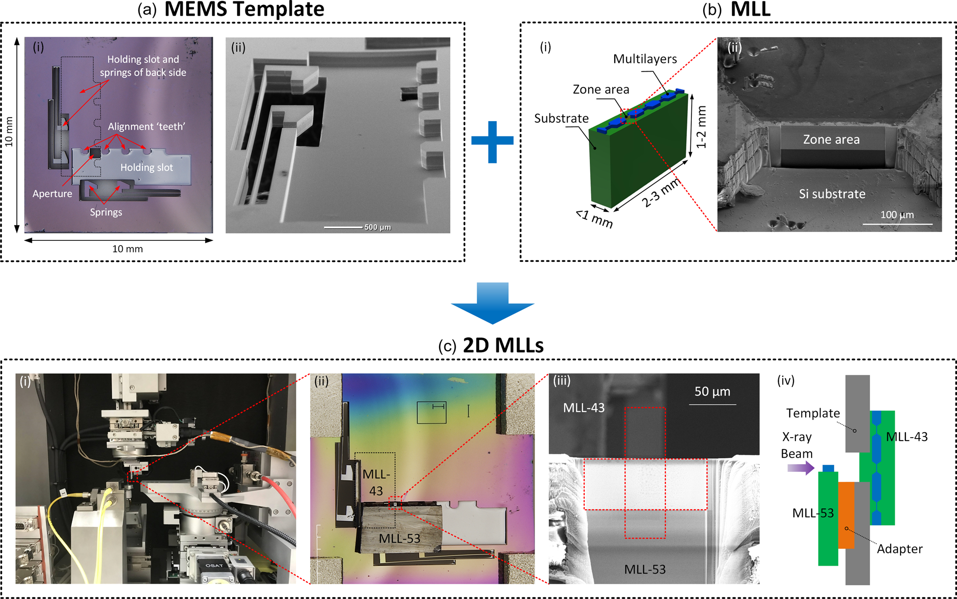
Figure 4: (a) Microfabricated MEMS template ((i) The optical image, (ii) SEM image of the holding slot). (b) MLL optics ((i) schematic of an MLL. (ii) SEM image of the focused ion beam (FIB)-etched zone area of the lens). (c) assembled 2D MLL optics ((i) the apparatus with mounted 2D MLL optics for X-ray focusing, (ii) 2D MLLs, (iii) overlapped zone areas, (iv) 2D MLLs configuration). Adapted with permission from [Reference Xu23] © The Optical Society.
MLL optics. Figure 4b-i shows the schematic of the fabricated MLL optics. The MLL optics typically have dimensions of 2–3 mm long, 1–2 mm high, and less than 1 mm thick. It includes a silicon substrate and deposited Si/WSi2 multilayers, in which there is a FIB polished zone area used for X-ray focusing. Figure 4b-ii shows an example of the FIB polished zone area of MLL optics. The two MLLs used in this work have aperture sizes (thickness of multilayer structure) of 53 μm (MLL-53) and 43 μm (MLL-43), respectively [Reference Xu23]. The thinnest zone is 4 nm for both lenses. The focal length for the upstream (MLL-53) and downstream (MLL-43) lenses is estimated to be around 5200 μm and 4200 μm, respectively, for 12 keV photon energy.
2D MLLs. Upon completion of the fabrication of MLL optics and MEMS templates, the 1D lenses were assembled onto the template. Figure 4c shows an example of 2D MLLs, which were mounted on a dedicated apparatus for X-ray focusing characterization [Reference Xu23]. There were two MLLs assembled on the template, one on each side. The positions of the zone area of the two lenses were adjusted to overlap each other under an optical microscope. The angular misalignment between two MLLs was determined to be ~6 millidegrees, and the separation distance between two MLLs was ~1050 μm.
X-ray focusing performance. The focusing performance of the developed 2D MLLoptics was evaluated at the Hard X-ray Nanoprobe (HXN) Beamline at the National Synchrotron Light Source II (NSLS-II) [Reference Nazaretski17]. The monolithic structure was mounted in a dedicated apparatus used for optics characterization [Reference Nazaretski15]. Ptychography was used for point-focus evaluation. The reconstructed line-focusing profiles for horizontal and vertical directions yielded the full width half maximum values of ~14 nm and ~13 nm, respectively, as shown in Figure 5a [Reference Xu23]. The inset in Figure 5a represents the reconstructed X-ray wavefront at its focal plane, with the phase shown in color and the amplitude in brightness. Since the majority of intensity is confined within the central peak with just modest side-lobes, the optics are ideal for direct (transmission or fluorescence) high-resolution imaging. Figure 5b demonstrates the absorption contrast (STXM) image produced by plotting the total transmission as a function of the sample (Siemens star) position. Figure 5c illustrates the amplitude of the simultaneous ptychography image for comparison. The 20 nm gaps between inner and outer spokes, which are the tiniest features, can be clearly resolved.
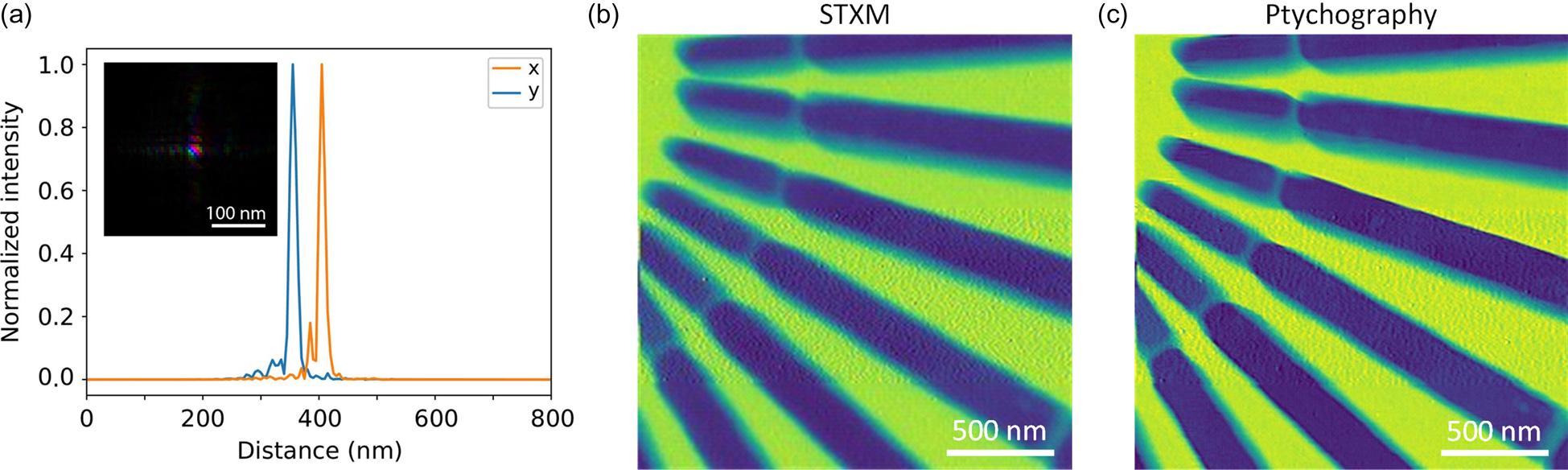
Figure 5: X-ray focusing performance of monolithic MEMS-based MLL optics. (a) Results of ptychography measurements. A point focus of ~14 nm and ~13 nm in horizontal and vertical directions has been reconstructed. The inset shows the shape of a probe with the amplitude being displayed with brightness and the phase with color. (b) Scanning transmission X-ray microscopy (STXM) image formed by plotting the total transmission as a function of sample position. (c) Ptychography (amplitude) image for the STXM measurement. The smallest features of 20 nm (gaps between inner and outer spokes) can be resolved. Adapted with permission from [Reference Xu23] © The Optical Society.
Discussion and Conclusion
The developed monolithic MEMS-based 2D multilayer Laue lens nanofocusing optics significantly simplify the MLLs alignment process and, meanwhile, guarantee the angular and lateral alignment of assembled 2D optics. At 13.6 keV photon energy, the X-ray ptychography measurements yielded astigmatism-free point focusing of ~14 nm and ~13 nm in horizontal and vertical directions, respectively. The new 2D optics remarkably reduce the complexity of current MLL microscopes and makes 2D MLLs compatible with conventional zone plate-based scanning X-ray microscopes. Any synchrotron facility that operates a zone plate-based microscope and is interested in high-resolution hard X-ray imaging will benefit from this new focusing device to improve imaging capabilities. The developed 2D MEMS-based MLL optic is a significant step forward in bringing robust, compact, user-friendly, high-resolution hard X-ray imaging capabilities to synchrotron and, potentially, lab-based X-ray microscopes.
Acknowledgments
This work was partially carried out at the Center for Functional Nanomaterials, Brookhaven National Laboratory and was supported by the U.S. Department of Energy, Office of Basic Energy Sciences, under Contract No. DE-SC0012704. Resources of the National Synchrotron Light Source II, a U.S. Department of Energy (DOE) Office of Science User Facility operated for the DOE Office of Science by Brookhaven National Laboratory under Contract No. DE-SC0012704, were utilized. This work was also performed in part at the Advanced Science Research Center NanoFabrication Facility of the Graduate Center at the City University of New York.


