


Introduction
The AlGaN materials system is attractive from the viewpoint of fabricating unipolar power devices because of its large bandgap and relatively high electron mobility. [Reference Shur1-Reference Pearton, Zolper, Shul and Ren6] An example is the use of Schottky diodes as high-voltage rectifiers in power switching applications. [Reference Chyi, Lee, Chuo, Chi, Dang, Zhang, Ren, Cao, Pearton, Chu and Wilson2-Reference Trivedi and Shenai4,Reference Pearton, Zolper, Shul and Ren6] These diodes will have lower blocking voltages than p-i-n rectifiers, but have advantages in terms of switching speed and lower forward voltage drop. Edge termination techniques such as field rings or field plates, bevels or surface ion implantation are relatively well-developed for Si and SiC and maximize the high voltage blocking capability by avoiding sharp field distributions within the device. [7] However in the few GaN Schottky diode rectifiers reported to date [Reference Chyi, Lee, Chuo, Chi, Dang, Zhang, Ren, Cao, Pearton, Chu and Wilson2,Reference Bandic, Bridger, Piquette, McGill, Vaudo, Phanse and Redwing3], there has been little effort made on developing edge termination techniques. Proper design of the edge termination is critical both for obtaining a high breakdown voltage and reducing the on-state voltage drop and switching time.
In this paper we report on the effect of various edge termination techniques on the reverse breakdown voltage, VB, of planar GaN Schottky diodes which deplete in the lateral direction. A maximum VB of 3.1 kV at 25°C was achieved with optimized edge termination, which is a record for GaN devices. We also examined the temperature dependence of VB in mesa diodes and found a negative temperature coefficient of this parameter in these structures.
Experimental
The GaN was grown on c-plane Al2O3 substrates by Metal Organic Chemical Vapor Deposition using trimethylgallium and ammonia as the precursors. For vertically-depleting devices, the structure consisted of a 1µm n+ (3×1018 cm−3, Si-doped) contact layer, followed by undoped (n=2.5×1016 cm−3) blocking layers which ranged from 3-11μm thick. These samples were formed into mesa diodes using Inductively Coupled Plasma etching with Cl2/Ar discharges (300 W source power, 40 W rf chuck power). The dc self-bias during etching was −85 V. To remove residual dry etch damage, the samples were annealed under N2 at 800°C for 30 secs. Ohmic contacts were formed by lift-off of e-beam evaporated Ti/Al, annealed at 700°C for 30 secs under N2 to minimize the contact resistance. Finally, the rectifying contacts were formed by lift-off of e-beam evaporated Pt/Au. Contact diameters of 60-1100μm were examined.
For laterally-depleting devices, the structure consisted of ∼3μm of resistive (107 Ω/-) GaN. To form ohmic contacts, Si+ was implanted at 5×1014 cm−2, 50 keV into the contact region and activated by annealing at 150°C for 10 secs under N2. The resulting n-type carrier concentration was 1×1019 cm−3. The ohmic and rectifying contact metallization was the same as described above.
Three different edge termination techniques were investigated for the planar diodes[7]: (i) use of a p-guard ring formed by Mg+ implantation at the edge of the Schottky barrier metal. In these diodes the rectifying contact diameter was held constant at 124μm, while the distance of the edge of this contact from the edge of the ohmic contact was 30µm in all cases.
(ii) use of p-floating field rings of width 5µm to extend the depletion boundary along the surface of the SiO2 dielectric, which reduces the electric field crowding at the edge of this boundary. In these structures a 10µm wide p-guard ring was used, and 1-3 floating field rings employed.
(iii) use of junction barrier controlled Schottky (JBS) rectifiers, i.e. a Schottky rectifier structure with a p-n junction grid integrated into its drift region. In all of the edge-terminated devices the Schottky barrier metal was extended over an oxide layer at the edge to further minimize field crowding, and the guard and field rings formed by Mg+ implantation and 1100°C annealing.
Results and Discussion
(a) Effects of Edge Terminations
Figure 1 (top) shows a schematic of the planar diodes fabricated with the p-guard rings, while the bottom of the Figure shows the influence of guard ring width on VB at 25°C. Without any edge termination, VB is ∼2300 V for these diodes. The forward turn-on voltage was in the range 15-50 V, with a best on-resistance of 0.8Ωcm2. The figure-of-merit (VB)2/RON was 6.8 MW·cm−2. As the guard-ring width was increased, we observed a monotonic increase in VB, reaching a value of ∼3100 V for 30μm wide rings. The figure-of-merit was 15.5 MW·cm−2 under these conditions. The reverse leakage current of the diodes was still in the nA range at voltages up to 90% of the breakdown value.
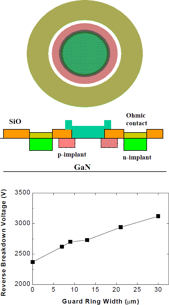
Figure 1. (top) View of rectifiers with p-type guard rings.(bottom) Variation of VB with guard ring width.
Figure 2 (top) shows a schematic of the floating field ring structures, while the bottom section shows the effect of different edge termination combinations on the resulting VB at 25°C. Note that the addition of the floating field rings to a guard ring structure further improves VB, with the improvement saturating for a 3 floating field ring geometry.
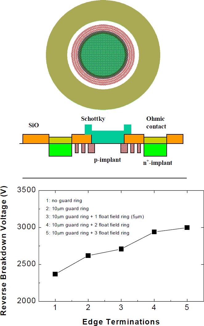
Figure 2. (top) View of rectifiers with floating field rings.(bottom) Variation of VB with or without a 10μm wide p-guard rings a 1, 2 or 3 floating field rings. The field ring width was 5μm in all cases.
Figure 3 shows the effect of the junction barrier control on VB, together with a schematic of the p-n junction grid. In our particular structure we found that junction barrier control slightly degraded VB relative to devices with guard rings and various numbers of floating field rings. We believe that with optimum design of the grid structure we should achieve higher VB values and that the current design allows Schottky barrier lowering since the depletion regions around each section of the grid do not completely overlap. This is consistent with the fact that we did not observe the decrease in forward turn-on voltage expected for JBS rectifiers relative to conventional Schottky rectifiers.
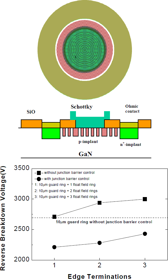
Figure 3. (top) View of rectifier with junction barrier control.(bottom) ariation of VB in devices with a 10μde p-guard ring and 1, 2 or floating field rings, either with or without junction barrier control.
The results of Figure 1-3 are convincing evidence that proper design and implementation of edge termination methods can significantly increase reverse breakdown voltage in GaN diode rectifiers and will play an important role in applications at the very highest power levels. For example, the target goals for devices, intended to be used for transmission and distribution of electric power or in single-pulse switching in the subsystem of hybrid-electric contact vehicles are 25 kV standoff voltage, 2 kA conducting current and a forward voltage drop <2% of the standoff voltage. At these power levels, it is expected that edge termination techniques will be essential for reproducible operation.
Summary and Conclusions
GaN Schottky diodes with vertical and lateral geometries were fabricated. A reverse breakdown voltage of 3.1 kV was achieved on a lateral device incorporating p-type guard rings. Several types of edge termination were examined, with floating field rings and guard rings found to increase VB. The best on-state resistance obtained in these lateral devices was 0.8Ωcm2 In mesa diodes incorporating n+ contact layers, the best onstate resistance was 6 mΩcm2, while VB values were in the range 200-550V. These GaN rectifiers show promise for high power electronics applications.
Acknowledgements
The work at UF is partially supported by an NSF grant (DMR-9732865, L. Hess) and by a DARPA/EPRI grant (D. Radack/J. Melcher), no. MDA 972-98-1-0006 monitored by ONR (J. C. Zolper). The work at NCU is sponsored by the National Science Council of R.O.C. under contract no. NSC-88-2215-E-008-012. The work of RGW is partially supported by a grant for ARO (J.M. Zavada). Sandia is a multiprogram laboratory operated by Sandia Corporation, a Lockheed-Martin company, for the US Department of Energy under grant DEAC04-94AL85000.


