Introduction
Great interest exists in the III-nitride semiconductors since the successful development in growth of GaN based materials and operation of electronic and optoelectronic devices such as blue and green light emitting diodes (LEDs) and laser diodes (LDs) [Reference Nakamura, Senoh, Iwasa and Nagahama1,Reference Nakamura, Senoh, Iwasa, Nagahama, Yamada and Mukai2,Reference Nakamura and Senoh3,Reference Nakamura, Senoh, Nagahama, Iwasa, Yamada, Matsushita, Kiyoku and Sugimoto4]. The formation of stable and reliable low resistance ohmic contacts to p-type GaN has been a problem in achieving good performance of those devices. For devices with large contact areas such as LEDs and LDs, the specific contact resistance ( ρc ) between 10−4 to 10−6 Ωcm2 is considered acceptable and for devices with smaller contact areas, values of ρc between 10−5 to 10−7 Ωcm2 are necessary [Reference Holloway, Kim, Trexler, Miller, Fijol, Lampert and Haas5]. Bilayer metal schemes such as Ni/Au and Pd/Au were studied by many groups [Reference Koide, Maeda, Kawakami, Fujita, Uemura, Shibata and Murakami6,Reference Trexler, Pearton, Holloway, Mier, Evans and Karlicek7,Reference Kim, Khim, Chae and Kim8]. These have been studied due to the stable electrical and thermal properties and the high work function which is one criteria to form low resistance Ohmic contacts to p-type materials.
The effects of cryogenic cooling after heat treatment on the formation of Ni/Au and Pd/Au contacts are presented in this paper. We also compare these effects on forming Ni/Au and Pd/Au contacts annealed in a combined O2/N2 gas ambient. High temperature annealing may degrade homogeneity possibly caused by spiking of metals between themselves or between metal and semiconductor due to the differences in thermodynamic properties of materials. Annealing was conducted in an oxygen and nitrogen mixed gas ambient as reported by Y. Koide et al. [Reference Koide, Maeda, Kawakami, Fujita, Uemura, Shibata and Murakami6]. This is to remove hydrogen atoms contained in Mg-doped GaN epilayers. Removing hydrogen atoms results in the increase of the hole concentration and decrease of the contact resistance. Annealing in nitrogen gas ambient is believed to avoid nitrogen vacancies which act as doners. We expected that cryogenic treatment would reduce disadvantages from the discrepancy in thermodynamic properties of materials during cooling the heated samples to give improved Ohmic behavior. With cryogenic treatment, the changes of electrical and structural properties have been examined.
Experiment
The metal contacts were made on GaN films grown by metalorganic chemical vapor deposition (MOCVD) on (0001) sapphire substrates. The GaN films consisted of the Mg doped p-type GaN with a thickness of 2µm on a 30nm thick GaN buffer layer. The hole concentration of the p-GaN layer was 1.41×1017 cm−3 and the resistivity was 3.5 Ωcm. The samples were sequentially ultrasonically cleaned in trichloroethylene, acetone and methanol, then rinsed in 18 MΩ de-ionized ( DI ) water. The cleaned samples were chemically etched in boiling aqua regia of HNO3 : HCl = 1 : 3 for 10 minutes to remove the native oxide and the contamination of the GaN surface as suggested by J. K. Kim et al [Reference Kim and Lee9]. Then, a photolithographic process was used to form the pattern for the circular transmission line method (c-TLM). In this pattern, the radius of the inner circular contact was 400 µm and the spacings between inner and outer circles ranged from 25µm to 75 µm. Prior to the deposition of metal, the sample was etched in a warm solution of HNO3 and HCl again. The warm solution means non-boiling aqua regia : a solution was boiled and cooled for 2∼3 minutes since very hot solution ruins the photoresist. The Ni ( 30nm) / Au (15 nm) and the Pd (25 nm)/ Au (15 nm) contacts were deposited by thermal evaporation and completed by liftoff. The contacts were then annealed at temperatures ranging from 400 to 700 °C for 10 minutes in a conventional furnace in an oxygen and nitrogen mixed gas ambient. In order to study the effect of cryogenic treatment, some samples were subsequently cooled by dipping in liquid nitrogen after the heat treatment, then brought to room temperature in air. Sister samples were not quenched in liquid nitrogen.
The current versus voltage (I-V) curves were measured as deposited and between each heat treatment interval. After each measurement of I-V curves, the specific contact resistance ( ρc ) was determined by use of the c-TLM. The samples with and without cryogenic treatment showing the lowest contact resistance were examined by scanning electron microscopy (SEM) images using a model Hitachi S-4000 and atomic force microscopy (AFM) images using a model Quesant Res/stg and electron spectroscopy for chemical analysis (ESCA) depth profiles using a model Surface Science SSX-100 with an ion energy of 4.5 keV, a raster size of 2×2 mm, a sputter time per step of 1∼2 min. and a x-ray spot size of 1000 µm.
Results
1. Electrical Properties
The current versus voltage curves for the as deposited, annealed and annealed plus cryogenically treated Ni/Au and Pd/Au contacts to p-GaN are shown in Figure 1. Annealed contacts shown in Figure 1 were treated in an O2/N2 ambient. For the as deposited case, both Ni/Au and Pd/Au contacts show similar behavior of non linear I-V with a small potential barrier. However, the Pd/Au contact reveals a lower specific contact resistance of 7∼10×10−4 Ωcm2 compared to 4∼6×10⁻² Ωcm2 for the Ni/Au contact in the linear region, although the work function of Ni (5.15 eV) is slightly higher than Pd (5.12 eV). These characteristics agree with previous studies [Reference Trexler, Pearton, Holloway, Mier, Evans and Karlicek7,Reference Kim, Khim, Chae and Kim8]. We believe that the lower contact resistance of the Pd/Au contact with lower work function of Pd is due to a new phase with higher work function which will be discussed from the ESCA profiles. The non linear I-V behaviors for both Ni/Au and Pd/Au contacts were improved by heat treatment at temperatures of 600 °C and 700 °C, respectively. The reduction of the specific contact resistances to 9.84×10⁻⁴ Ωcm2 for Ni/Au and 1.80×10⁻⁴ Ωcm2 for Pd/Au were also obtained by heat treatment. Lowering the contact resistance and improving linearity may come from a more intimate contact of metal with semiconductor or any new phases having higher work function. Intimate contact leads to more current flow across the interface by breaking up some of the interfacial contamination between metal and semiconductor. Possible new compounds reduce the potential offset at the metal/ semiconductor interface by forming a layer of a compound with higher work function or causing a highly doped region. In contrast, the effect of cryogenic treatment on forming those two contacts is quite different. With further treatment by cooling in liquid nitrogen after the anneals, the Ni/Au contact exhibits better linearity of I-V characteristics and a contact resistance of 2.65×10⁻⁴ Ω cm2. However, the Pd/Au contact show opposite behavior to the Ni/Au contact such that cryogenic treatment degrades the specific contact resistance value to 3.34×10⁻⁴ Ω cm2. The effect of cryogenic treatment on improving Ohmic behavior could be caused by some of the semiconductor dissolving in the metal on heating and recrystallization with a high concentration of the electrically active element in solid solution on subsequent cooling [Reference Rhoderick and Williams10]. It could also be due to improved morphology as explained later. Therefore, the mechanisms and the reactions at the interface between metal and semiconductor for Ni/Au contact and Pd/Au contact would be different.
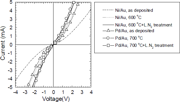
Figure 1. Current versus voltage curves for the Ni/Au and the Pd/Au contacts to p-GaN as deposited and annealed with and without cryogenic treatment in liquid nitrogen.
2. Structural properties
Figure 2 shows ESCA depth profiles of Ni/Au contacts heated in O2/N2. The ESCA depth profile for the as deposited sample of the Ni/Au contact shows the abrupt and sharp signals corresponding to the interfaces of the Au/Ni/GaN and all of the species ( Au, Ni, Ga and N ). From the ESCA depth profile, there is no evidence of interdiffusion from deposition alone. However, ESCA profiles change in behavior with annealing and cryogenic treatment. In the ESCA profile of an annealed sample, Figure 2(a), Ni diffused to the surface of the contact and into the GaN. The O signal follows the Ni signal, which indicates a NiO phase. This is evident from chemical analyses, which show core levels of Ni 2p3/2 and NiO at the binding energies of 852.6 eV and 854.7 eV, respectively. On the other hand, Au exchanges position with Ni and forms an intimate contact with the GaN layer. These results agree with previous reports in which Ni diffused through the Au capping layer to the surface of the contact where it oxidized [Reference Trexler, Pearton, Holloway, Mier, Evans and Karlicek7]. A similar behavior in ESCA depth profiles is also shown for the annealed plus cryogenic treated sample as in Figure 2(b). Our study indicates that the direct contact to GaN would be a combination of NiO and Au. Y.Koide et al. by using x-ray diffraction (XRD) reported a NiO layer and no evidence of interaction between metals and GaN for the Ni/Au contacts annealed in an O2/N2 ambient [Reference Koide, Maeda, Kawakami, Fujita, Uemura, Shibata and Murakami6]. On the other hand, H.S.Venugopalan et al. [Reference Venugopalan, Mohney, Luther, Delucca, Walter, Redwing and Bulman11] found a NiGa phase for the annealed Ni/n-GaN scheme and J.T.Trexler et al. [Reference Trexler, Miller, Holloway and Kwan12] reported the possibility of a Ni-N solid solution for the annealed Ni/Au scheme.
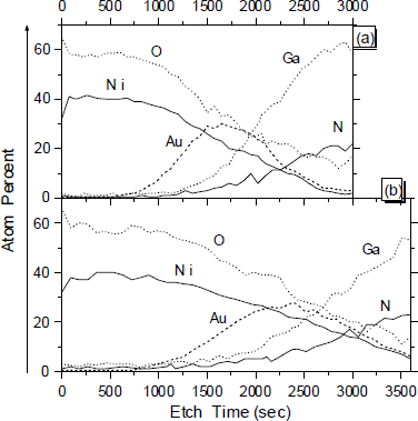
Figure 2. ESCA depth profiles for the Au/Ni/p-GaN: (a) annealed at 600 °C 10 min. in O2/N2 and (b) annealed and cryogenically treated.
The ESCA depth profiles of Pd/Au contacts are shown in Figure 3. For both contacts annealed and cryogenic treated in addition to annealing, there is no evidence of formation of PdO but of Au:Pd solid solution. This new phase ( Au:Pd solid solution ) was reported by other groups [Reference Koide, Maeda, Kawakami, Fujita, Uemura, Shibata and Murakami6,Reference Trexler, Pearton, Holloway, Mier, Evans and Karlicek7]. The Ga and N signals tail out and extend out to the surface, which might indicate the decomposition of the GaN matrix. No significant difference was seen between the samples only annealed and annealed plus cryogenic treated. Note that the published sputter rate for Pd is 100 nm/min. compared to 60 nm/min. for Ni.

Figure 3. ESCA depth profiles for the Au/Pd/p-GaN: (a) annealed at 700 °C 10 min. in O2/N2 and (b) annealed and cryogenically treated.
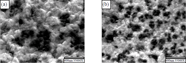
We also examined surface morphology of those contacts using SEM. The SEM images of the as deposited samples for Ni/Au and Pd/Au contacts show a smooth metal surface. However, Figure 4 for the Ni/Au contact shows the change in the surface morphology of samples annealed ( Figure 4(a) ) and cryogenic treated ( Figure 4(b) ). It clearly shows bright and gray particles within a deep dark area. From a comparison with composition vs. depth in ESCA profiles, the bright and gray particles are NiO and black areas would be the mixing of the transition metal oxide ( NiO ) and Au which directly contacts with GaN. Figure 4(b) shows that the cryogenic treated sample has a smaller dark area (black) and smoother surface of NiO ( bright and gray ) than the other (Figure 4(a)). For the Pd/Au contacts in Figure 5, we can see a difference in particle size but not in roughness. The sample not cryogenic treated, in Figure 5(a), has non uniform larger particles. Contrary to this feature, the sample with liquid nitrogen cooling shows almost uniform particles. We believe that the “balling-up” of the NiO layer occurs during the heating process from the compressive stress due to the difference of the thermal expansion coefficients between Ni (13.3×10⁻⁶ K−1) [Reference Brandes13], Au (14.1×10⁻⁶ K−1) [Reference Brandes13], Pd (11×10−6 K−1), and GaN (6×10⁻⁶ K−1) [Reference Duxstad, Haller, Yu, Hirsch, Imler, Steigerwald, Ponce and Romano14]. The differences in surface features for the contacts with and without cryogenic treatment are in size and thickness of the different colored regions. In addition to the effect of compressive stress, strain is also induced during cooling due to the difference of thermal expansion coefficients of materials. Therefore, we suggest that subsequent and fast cooling in liquid nitrogen minimizes the effect of compressive stress and strain, then results in the laterally more uniform surface which is significant in the electrical properties. This is supported by AFM data which show the surface roughness of the Ni/Au contact. The average values of the surface roughness are 64.78 nm and 37.38 nm for the contacts annealed only compared to those treated in liquid nitrogen after annealing, respectively. There is no much difference in the values of the surface roughness : 54.46 nm for annealed and 68.2 nm for annealed plus cryogenic treated, for the Pd/Au contacts from the AFM images.

Figure 4. SEM images for the Ni/Au contacts to p-GaN: (a) annealed at 600 °C for 10 min. in an O2/N2 and (b) annealed and cryogenically treated.
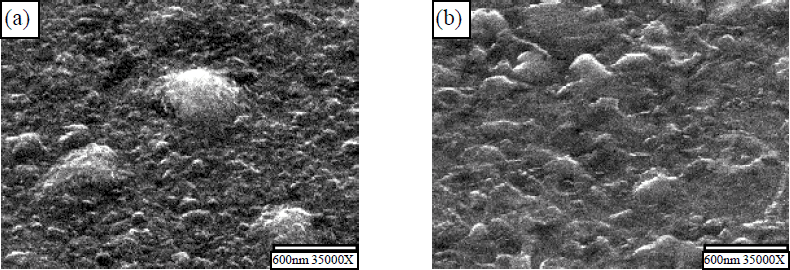
Figure 5. SEM images for the Pd/Au contacts to p-GaN: (a) annealed at 700 °C for 10 min. in an O2/N2 and (b) annealed and cryogenically treated.
Conclusions
Both Ni / Au and Pd/Au contacts to p - GaN show Ohmic behavior with and without a cryogenic treatment. The cryogenic treatment on the Ni/Au contacts improves the I-V linearity and reduces the specific contact resistance from 9.84×10⁻⁴ Ωcm2 to 2.65×10⁻⁴ Ωcm2. The phases NiO and Au:Pd have been observed for both contact systems, respectively. Subsequent and fast cooling in liquid nitrogen after anneal affects the recrystallizing of NiO and Au:Pd solid solution produced from heat treatment, then improves surface morphology. The contact resistance is improved by: i) heat temperature which forms new phases at the GaN surface compared to the initial deposit; and ii) cryogenic treatment which affects both the recrystallization and surface morphology.