


The editors of Microscopy Today congratulate the winners of the tenth Microscopy Today Innovation Award competition. The ten innovations described below advance microscopy in several areas: light microscopy, electron microscopy, and scanning probe microscopy. These innovations will make microscopy and microanalysis more powerful, more productive, and easier to accomplish.
Access™ Atomic Force Microscope
Angstrom Science, Inc.
Developers: Andy Erickson, Stephen Ippolito, and Kyle Hofstatter
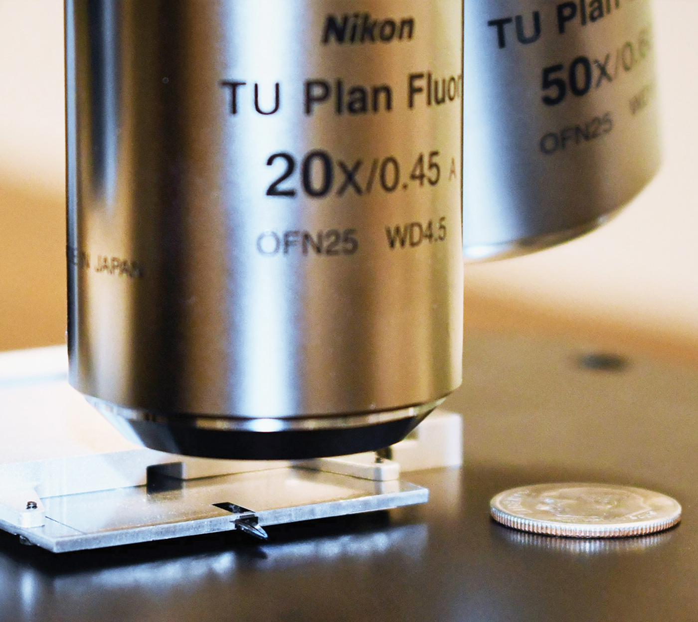
A thin atomic force microscope (AFM) has been designed to be integrated with commercial light microscopes employing high numerical aperture (NA) objective lenses that have inherently short working distances. Integration with the a flexible research light microscope permits rapid finding of the area of interest for detailed AFM studies.
The new AFM scanning head is roughly two orders of magnitude smaller than a conventional AFM head. This is accomplished using a patented technique in which a laser beam from a single-mode fiber is refracted by a graded-index multi-mode fiber that serves as a lens to focus the beam onto the cantilever. This beam is reflected back into the same optical fiber and transported to a position-sensitive photo detector. The length of the single-mode fiber to the controller can be extended without degradation of either the incident or reflected beam, therefore the light source and detector optoelectronics can be placed in the AFM controller rather than near the cantilever. This removes a major source of heat from the AFM head. In addition, the small mass and size of the Access™ AFM design, along with a shortened mechanical feedback loop, makes the AFM less susceptible to noise and drift, enabling sub-Angstrom noise performance.
The Access™ combined with a light microscope eliminates the need for time-consuming large area scans, used with traditional AFMs to find the area of interest. The light microscope provides search capabilities at several magnifications. The smaller, thinner design of the AFM head permits the use of light microscopy objectives with shorter working distances and higher numerical aperture (NA), thereby improving both light microscopy image resolution and signal collection efficiency. The long-working-distance requirements of most commercial AFMs cause the typical light microscope 20× objective to have a low NA of ~0.3 and a resolving power of only about 1 µm. The Access™ AFM allows high-NA, diffraction-limited light microscopy with light microscopy resolution about 200 nm. The AFM provides nanometer-level lateral image resolution plus force spectroscopy to reveal mechanical properties and other modes for measuring electrical characteristics and magnetic forces. This thin AFM design may even improve the efficiency of tip-enhanced Raman spectroscopy (TERS).
Compact Quadrupole-Based Ultrafast Mev Transmission Electron Microscope
Brookhaven National Lab, ShanghaiTech University, and City University of Hong Kong
Developers: Yimei Zhu, Weishi Wan, and Fu-Rong Chen
This new design of an MeV ultrafast transmission electron microscope (TEM) is based on combinations of compact, low-cost quadrupoles. The magnetic quadruple lens with asymmetric focusing is used to focus high-energy electrons in accelerators. It is challenging to adapt quadrupoles for illumination and imaging tasks in electron microscopes, however groups of quadrupoles (multiplets) can form a lens with desirable properties, such as rotational symmetry and a focal length that is tunable. The concept of using quadrupole quintuplets as electron imaging lenses, originally proposed by Harald Rose, is now being implemented in a 3 MeV TEM at Brookhaven National Laboratory.
High-energy relativistic electrons can minimize space charge for ultrafast microscopy, but traditional round lenses to focus such electrons are bulky and expensive. The present design consists of various quadrupole-based multiplets arranged to achieve a higher degree of symmetry, to reduced aberrations, and to obtain better performance in MeV microscopes. This design has never been implemented, but a systematic study shows that by taking into account aberrations up to 5th order, a 4 Å (0.4 nm) image resolution is achievable using a radio frequency (RF) electron source. With a field-emission electron source, resolution should be further improved.
The repulsive force between two electrons decreases with increased electron velocity and energy. Thus, MeV electrons can improve the temporal resolving power of a microscope by reducing the space charge. In addition, compared with low-energy electrons, high-energy electrons penetrate thicker samples and yield better contrast transfer functions for imaging. The short electron wavelength also offers opportunities for probing higher-order diffraction phenomena which are sensitive to atomic positions and phonons. A traditional MeV microscope occupies a 5-story building and costs about $50M. In contrast, the quadrupole-multiplet microscope is only about 1 meter long (or high) and can fit into a typical laboratory room.
Ultrafast electron microscopy has been identified as a major future direction for modern electron microscopy. Ultrafast MeV electron microscopy offers an opportunity for understanding the structural dynamics and behavior of matter under conditions far from equilibrium. Applications include direct observations of the fundamental processes that drive the functionalities of chemical, materials, and biological systems.
Electron Microscope Pixel Array Detector
Cornell University
Developers: David A. Muller, Sol M. Gruner, Mark W. Tate, Hugh T. Philipp, Katherine S. Shanks, Prafull Purohit, Kayla X. Nguyen, Zhen Chen, and Yi Jiang
The electron microscope pixel array detector (EMPAD) is a high-speed, high-dynamic-range pixelated direct electron detector with single-electron sensitivity and an unparalleled detective quantum efficiency over its operating range of 20 to 300 keV. It is intended for use as a quantitative, momentum-resolved detector for scanning transmission electron microscopy (STEM). The detector has a 1,000,000:1 dynamic range, a noise level of less than 1/100th of a primary electron at 200 keV, and a linear signal up to a few pA per pixel, and it can read out a full frame in under 1 ms. It can record a full unsaturated diffraction pattern containing intensity variations in the central disk simultaneously with details of higher order Laue zones suitable for quantitative analysis. This performance is enabled by a hybrid digital/analog readout design, with dedicated signal processing hardware operating simultaneously for each pixel. A large chip area (3.7 cm2) with large pixels ensures a good point spread function across the full range of primary beam energies. Key to the detector's performance is its high dynamic range, enabling it to record all features of a diffraction pattern, from an unsaturated central beam to single electrons at the highest scattering angles, and to do so without compromising recording speed or sensitivity. The detector can record all elastic imaging modes simultaneously.
The ability to record a full diffraction pattern from an atomic-sized electron beam has enabled ptychographic reconstructions to reach 2.5× beyond the diffraction limit of the electron microscope. By correctly phasing the overlap of diffracted beams, ptychography creates a virtual numerical aperture limited by the largest recorded scattering angle, rather than the incident convergence angle. This has boosted the resolution of an aberration-corrected STEM operating at 80 keV from 0.98 Å down to 0.39 Å, achieving a new world record for image resolution by any imaging method.
This system is well suited to mapping grain structure and strain distributions with sub-pm precision and imaging electric and magnetic fields, even in the presence of grain contrast. For ptychography, not only is the resolution limit of the microscope extended beyond the diffraction limit, but data acquisition is more dose-efficient than with conventional imaging modes. A commercial version is available through Thermo Fisher’s electron microscope division.
K3™ IS Direct Detection Camera
Gatan, Inc.
Developers: Sander Gubbens, Matt Lent, Paul Mooney, Cory Czarnik, Peter Denes, and Stephen Mick
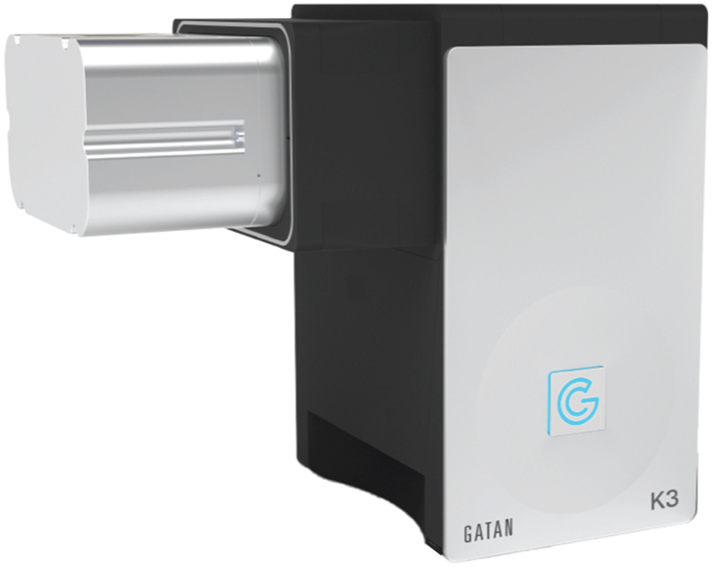
The K3 IS camera performs electron counting and continuous data acquisition at a data rate (in Gpix/sec) that is five times faster than any direct detection camera that has come before it. Similar to the industry-leading K2® camera, the K3 IS uses a direct detection complementary metal–oxide–semiconductor (CMOS) detector to identify and record individual electron events (that is, electron counting). Although the K2 camera offered an in situ image capture mode, the in situ mode did not take full advantage of electron counting. Instead, the K2 IS used a traditional linear accumulation to determine the grayscale value of each pixel in an image. By contrast, the K3 IS provides an in situ, continuous data acquisition mode that counts electron events in every pixel, in real time. Moreover, the K3 IS camera uses a new proprietary 23.6-megapixel sensor to capture 27.4 times the field of view of the K2 IS. The K2 IS acquisition mode required the K2 sensor to be binned 2×, but the K3 IS can acquire in situ images at the full field of view without binning.
The K3 IS stores data directly to disk in DigitalMicrograph® (*.dm4) software format, making it immediately accessible for processing and analysis. This approach to data storage, having the data directly readable, overcomes a major limitation of the K2 IS. That is, the K2 IS stored data as an intermediate format that was striated across four computer systems. To review an image from the K2 IS, the data would have to be reconstructed frame-by-frame. The K3 IS now allows data to be reviewed continuously, in real time, providing feedback at the transmission electron microscope (TEM) during an ongoing experiment. This capability can be used to great advantage to help guide experimental decision making at the microscope during a TEM session.
Applications of the K3 IS camera include catalysis, zeolite imaging, battery materials, and nanoparticle synthesis. The K3 IS camera will preserve image quality through its high detective quantum efficiency (DQE) while allowing dynamic reactions in these energy materials to be investigated both at sub-millisecond time scales and at low dose rates to greatly minimize the effects of the electron beam.
Nanoscale Tweezers for Single-Cell Biopsies
Imperial College London, Department of Chemistry
Developers: Joshua B Edel, Aleksander P. Ivanov, Binoy Paulose Nadappuram, and Paolo Cadinu
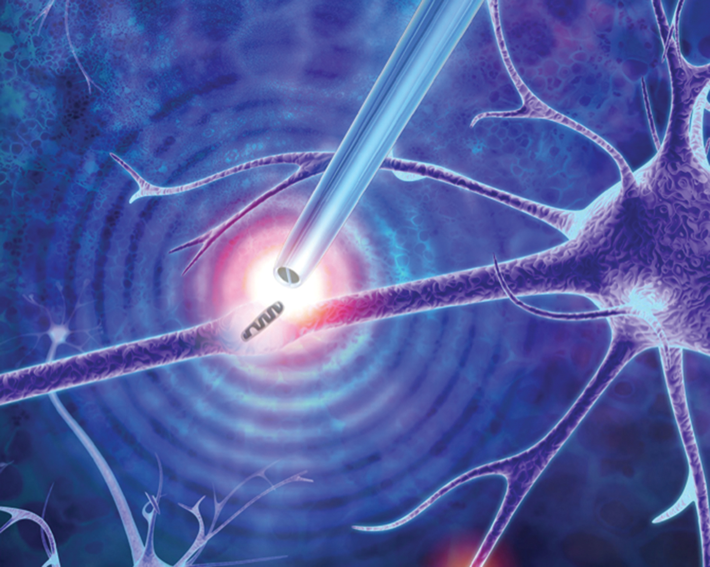
This microscopy technique employs a dielectrophoretic nanotweezer to trap, manipulate, and extract biomolecules and organelles in living cells. While our knowledge of how cells function is rapidly expanding, many unanswered questions remain. This is especially true for individual cells of the same type (such as brain, muscle, or fat cells) that have different compositions at the single-molecule level. Cataloging the diversity of seemingly identical cells can help researchers better understand cellular processes, design improved models of disease, and devise new patient-specific therapies. However, traditional methods for studying these differences typically involve bursting the cell, resulting in the loss of spatial information within the cell and dynamic information such as molecular changes in the cell over time.
The invention described here is a minimally invasive nanotweezer that can extract and manipulate a sample from living cells with single-molecule precision. These nanotweezers use dielectrophoresis (DEP) to trap molecules subjected to a non-uniform electric field. The device is composed of two individually addressable nanoelectrodes separated by a 10–20 nm insulating septum. A low voltage between the nanoelectrodes generates exceptionally high electric fields, which are capable of trapping and manipulating individual nucleic acids and proteins at physiological conditions. This allows the extraction of nucleic acids and organelles from living cells, including directly from the nucleus or the cytoplasm, for gene expression analysis.
These nanotweezers are inexpensive to fabricate, have a small footprint, and are robust in design. In sampling from a single cell, the process does not involve the withdrawal of cytoplasmic fluid and allows for the preconcentration of analyte in real time. This technique is especially useful for detection of molecular species present in low copy numbers, which is currently not possible with other state-of-the-art methods. This method offers the capability of non-destructive single-organelle manipulation within living cells, which is unprecedented.
Although the nanotweezer is a standalone device, its capabilities are fully exploited when operating in conjunction with other microscopy techniques such as the following: tracking protein expression inside the same cell in response to biochemical or mechanical stimuli, imaging the structure of a specific extracted protein or molecule, and manipulation of biomolecules for bottom-up fabrication of nanostructures.
AICrystallographer
Oak Ridge National Laboratory
Developers: Maxim Ziatdinov, Suhas Somnath, Stephen Jesse, Ondrej Dyck, Andrew R. Lupini, Sergei V. Kalinin, and Rama K. Vasudevan
AICrystallographer is a set of open-source, deep-learning- based workflows implemented in the form of Jupyter notebooks and available via the PyCroscopy domain on GitHub. AICrystallographer is designed for rapid translation of atomically resolved scanning transmission electron microscopy (STEM) images and movies into the coordinates of individual atoms and defects. AICrystallographer does not require long-range periodicity or uniform resolution, is insensitive to the presence of regions of amorphous phases and holes, does not require human oversight or input, and offers performance far exceeding the limits of human vision. AICrystallographer contains tools for the construction of atomic trajectories as well as point-defect and extended-defect libraries. It contains the following units: (1) DefectNet: for locating atomic defects in electron microscopy movies with a convolutional neural network using only a single movie frame to generate a training set; (2) AtomNet: a convolutional neural network for locating atoms in noisy experimental STEM data; (3) FerroNet: machine learning and multivariate analysis tools (neural networks, dimensionality reduction, clustering/unmixing) for analysis of ferroic distortions in high-resolution STEM data of perovskites; (4) SymmetryNet: a deep convolutional network used to determine 2D Bravais lattice symmetry from atomically resolved images; and (5) Tutorials: tutorial-like notebooks describing how to apply these techniques on your own.
As is usual for open-source code, it can incorporate developments from other groups, that is, outputs of AICrystallographer can be readily used for custom analysis (strains, etc.). AICrystallographer can be deployed as plug-ins in the Nion Swift environment and can be further extended to other Python interfaces for commercial STEMs as they become available. These analytical toolboxes can be used both online (from within microscope control software) and offline (for post-acquisition data analysis), and the package includes dynamic networks for real-time denoising and drift correction.
Electron microscopy has been experiencing a revolution in the volume, quality, and veracity of the structural and functional data it provides. The bottleneck now is a lack of fully automatic analysis tools that can process multiple images and even movies to condense the information into material-specific descriptors, identification and classification of atoms, and generation of libraries of structural elements akin to X-ray spectra libraries. AICrystallographer enables such fully automated analysis.
Atmosphere Catalysis Solution
Protochips, Inc.
Developers: Stamp Walden, Dan Gardiner, Mark Uebel, David Nackashi, and John Damiano
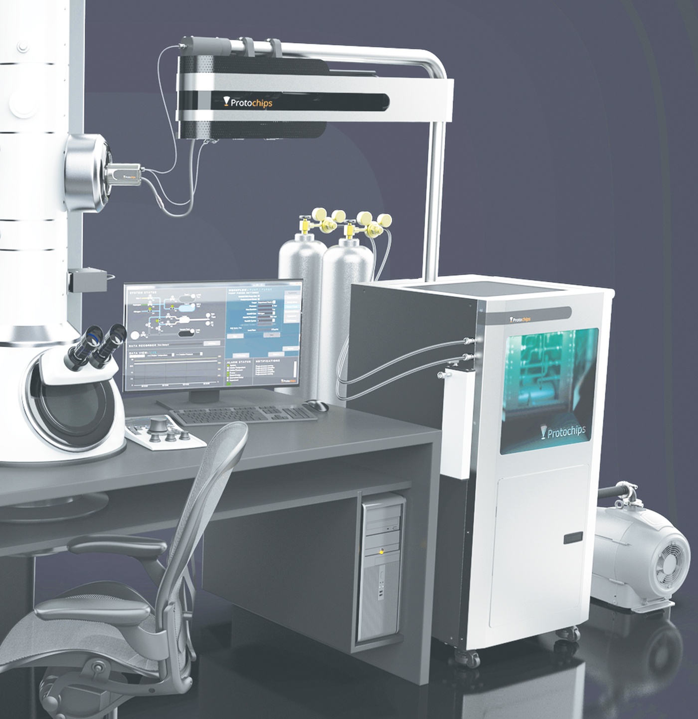
The Atmosphere Catalysis Solution is the first commercial in situ environmental TEM system with an integrated mass spectrometer and flexible gas handling system specifically designed for catalyst materials research. This product enables researchers to study how a catalyst's typical operating environment affects its efficiency, selectivity, and life span. The system includes a closed-cell TEM holder, custom gas handling manifold, vapor introduction kit, and an integrated residual gas analyzer (RGA) mass spectrometer.
Researchers can create a realistic operating environment for a catalyst within the closed-cell holder between two micro-electrical mechanical systems (MEMS) devices that form a mini reactor. The environmental controls include gas composition, pressure, flow rates, and heat. The custom gas handling manifold is designed to measure, mix, and flow gases using Dalton's law of partial pressures, rather than mass-flow controllers. This provides a wider range of gas flexibility including vapors such as water, alcohols, and organics. Environments are created with up to 1 atmosphere of pressure and up to 1000°C using a patented silicon carbide heating membrane. Experimental parameters are set using Protochips Clarity software that allows control of each environmental parameter independent of the others. The software also enables automated overnight cleaning cycles and bake-outs.
On the outlet side of the closed-cell holder is an integrated RGA system that verifies reaction gases prior to beginning an experiment, measures reaction products, and monitors the cleanliness of the gas handling system. The RGA is mounted on the boom of the system to maximize speed of gas detection, decreasing detection time to less than 3 seconds as compared to “external” RGA systems, which take up to 15 seconds. Integration also allows the RGA's high-vacuum environment to be supported by the high-vacuum environment already in Atmosphere's manifold, eliminating the need for the noisy diaphragm pump that compromises imaging resolution yet is required with any other mass spectrometry system. Protochips Clarity software has safety features to allow even inexperienced users to operate the system. With the Atmosphere Catalysis Solution, researchers can precisely vary relevant environmental conditions and observe how they affect not only the atomic structure but also the reactivity of the catalyst, for example, identifying conditions that can lead to deactivation.
HT-2 Holotomographic Microscope With 3D Fluorescence
Tomocube, Inc.
Developers: Y K Park, Sangchan Na, and Taehong Kim
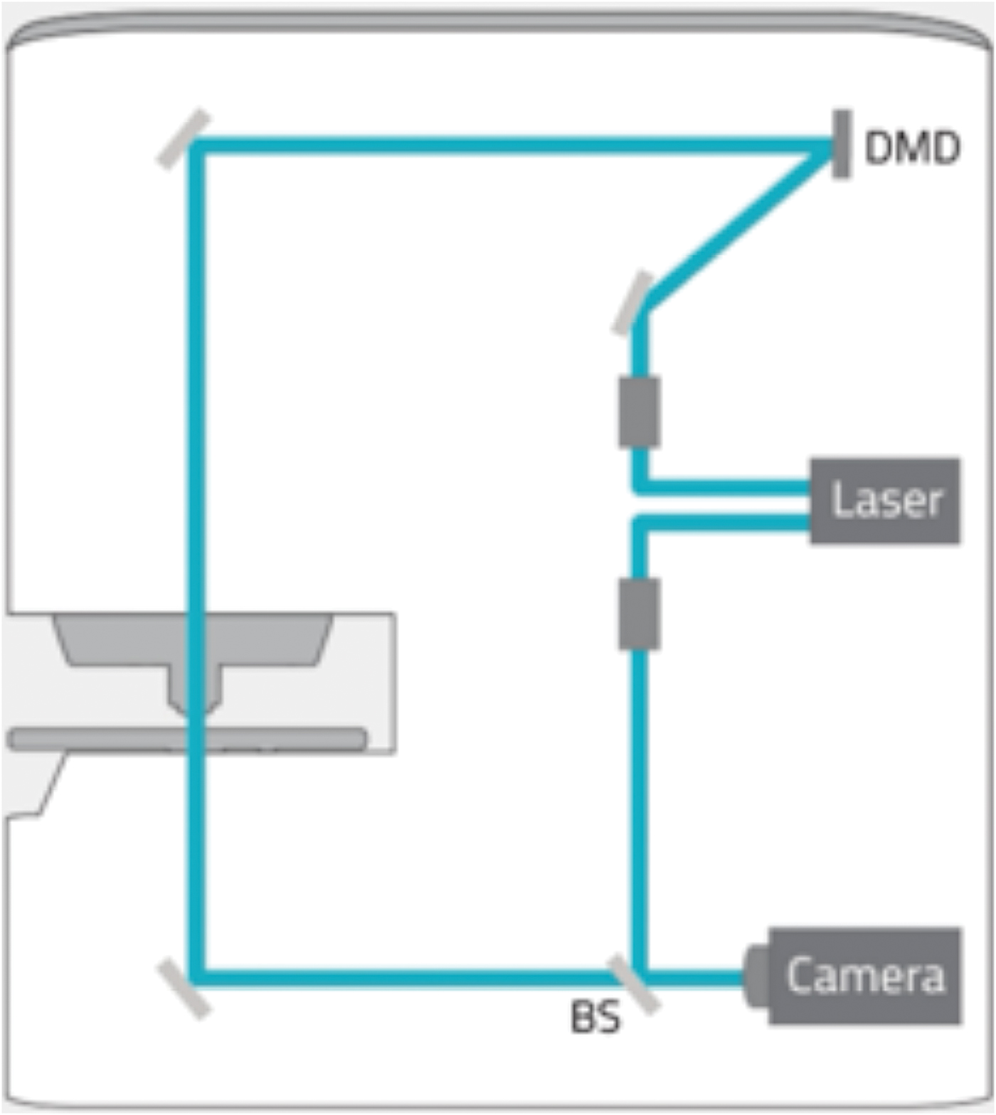
Holotomography (HT) is a three-dimensional quantitative phase imaging (QPI) technique using laser interferometry to provide label-free 3D imaging of live cells and tissues. As a light microscopy analog of X-ray computed tomography (CT), HT measures multiple 2D holograms of a sample acquired at various illumination angles from which the 3D refractive index (RI) distribution of the sample may be reconstructed by inversely solving the wave equation.
A laser light source of 532 nm is attenuated to below 1% output energy, and the beam feeds into two optical paths, an imaging path and a reference path. Light in the imaging path is expanded to fill the reflector area of a Texas Instruments digital micro-mirror device (DMD). The DMD can be directed to create a mirror pattern which can rotate the beam around the optic axis, through 360 degrees at an angle of 53 degrees, to acquire the data for reconstruction (48 images of 1k × 1k in 0.4 seconds). Each data set from the sample is combined with the reference beam, to create 2D interferograms from which the refractive index is calculated for each voxel in the image. Image data are “super-resolved” with voxels of about 120 nm × 120 nm × 240 nm. Selected bands of refractive index can be pseudo-colored to highlight structures within the cell. While HT can highlight cell morphology, it does not offer the specificity of fluorescence labeling. However, the combination of 3D HT with 3D fluorescence (FL) microscopy on the HT-2 allows the user to obtain 3D specificity and then track features/structures in time without using the high-intensity FL light source that could damage cells.
The HT microscope allows cell morphology to be tracked, monitored, and measured without labeling. Where cells contain high refractive index components (lipids in hepatocytes or nanoparticles), these can be detected, segmented, and evaluated. There is no modification of the cell which might affect its morphology, development, or behavior. Perpetual cell lines can be imaged without a label and without phototoxic effects. This is of particular importance where cells may be later reintroduced into organisms. as in the case of stem cells or perhaps modified T-cells.
Secondary Electron Electron-Beam-Induced-Current (SEEBIC) Imaging
University of California at Los Angeles
Developers: Chris Regan and William Hubbard
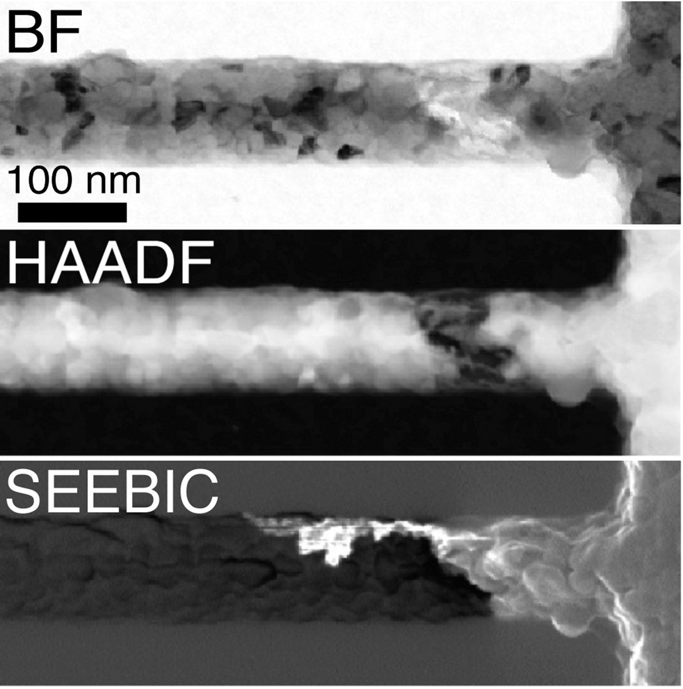
While intimately related to prior electron-beam-induced-current (EBIC) methods in the SEM, secondary electron electron-beam-induced-current (SEEBIC) imaging is qualitatively and quantitatively different. What makes the SEEBIC system new is that both the secondary electron (SE) and hole signals are detected in a scanning transmission electron microscope (STEM).
SEEBIC differs from traditional EBIC in several ways. The measuring circuits are wired differently. In the former case the end of the device remote from the transimpedance amplifier is extremely high impedance, while in the latter it is tied to a low impedance (usually ground) to allow charge neutralization. While traditional EBIC imaging is sensitive to holes, it only generates contrast in regions where the sample supports an electric field that will separate electron-hole pairs. In most samples such regions are special and localized, for example, in a p-n junction. Thus, most of the sample generates no contrast when imaged with traditional EBIC. SEEBIC, on the other hand, is an inevitable consequence of imaging a thin specimen with an energetic electron beam, and SEEBIC imaging generates contrast everywhere in a sample.
SEEBIC imaging has not been demonstrated previously for a couple reasons. First, the typical SEM sample is electron-opaque, and primary beam absorption produces a large background; thus, the SEEBIC signal is buried in the noise of the traditional SEM EBIC apparatus. This background is largely absent in the electron-transparent samples used in STEM. Secondly, the secondary electron (SE) yield drops with increasing beam energy; therefore, the SE signal is even smaller in a 200 kV STEM than in a 30 kV SEM. Detection of the signal requires a current measuring system that is low-noise and protected from electromagnetic interference (1 pA EBIC corresponds to ~6,000 electrons in a 1 ms dwell time).
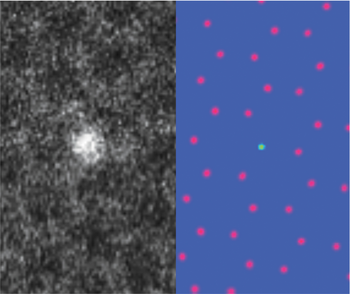
SEEBIC is sensitive to electric potential, electric field, work function, conductivity, and temperature, and it can probe these quantities with atomic resolution in a modern STEM. STEM SEEBIC can image a functioning resistive random access memory (RRAM). For example, in a HfO2-based RRAM, the conducting filament is thought to consist of oxygen vacancies. Oxygen vacancies are basically invisible in a standard STEM image, but they give excellent contrast when viewed with STEM EBIC imaging.
Single-Shot Label-Free Autofluorescence Multiharmonic (SLAM) Microscopy
University of Illinois at Urbana-Champaign
Developers: Stephen A. Boppart, Haohua Tu, and Sixian You
Single-shot, label-free autofluorescence multiharmonic (SLAM) microscopy achieves real-time, functional, and structural imaging; it enables a richer visualization of living systems. This nonlinear light microscopy can acquire images at subcellular resolution and at a relatively large depth with plausible endogenous contrasts indicative of authentic biological and pathological states. New laser source technology enables real-time acquisition of multiple endogenous molecular contrasts under one excitation condition to segment a rich set of cellular and extracellular components. Its single-beam, single-shot excitation and simultaneous multi-contrast epi signal detection allows this platform to avoid issues that have limited in vivo nonlinear optical molecular imaging in the past: perturbative sample pretreatments such as fluorescent labeling and mechanical sectioning, scarce or interdependent contrast generation, constraints on sample geometry, and intra-imaging motion artifacts.
The SLAM nonlinear imaging platform uses a custom-designed excitation laser at 1110 nm and ultrafast pulses at 10 MHz to enable fast single-shot acquisition of autofluorescence (FAD and NADH) and second/third harmonic generation from a wide array of cellular and extracellular components in living tissue (for example, tumor cells, immune cells, vesicles, and vessels). The unconventional choice of 1110 nm is what enables the simultaneous multiphoton excitation of autofluorescence from both FAD and NADH, as well as THG and SHG. Lower quantum yield at this longer excitation wavelength was overcome by employing a customized photonic crystal fiber source, producing coherent ultrashort pulses with a 60 nm wide spectrum and a 10 MHz repetition rate. Unlike marker-based intravital imaging approaches, the intensity of each channel in SLAM microscopy is proportionally correlated with the concentration of the auto-fluorophore or the arrangement of the molecular structures. Four channels acquire separate optical signatures that can be quantified to objectively describe metabolic and structural properties of individual cells and thus identify cellular and extracellular components. The method uses only 14 mW of incident power, which allows extended time-lapse investigations.
The single-source, single-excitation configuration of SLAM microscopy allows straightforward clinical translation to flexibly access deep tissue sites by a miniature (laparoscopic) microscope objective or fiber-based endoscope. This method has demonstrated its potential in vascular biology by differentiating rare recruited leukocytes among numerous flowing red blood cells.
