Introduction
III-V nitrides, SiC and diamond, are very promising materials for electronic devices that can operate under high-temperature, high-power, and high-frequency conditions [Reference Chow and Tyagi1], since these materials have a high melting point, a wide bandgap, a high breakdown electric field, and a high saturation velocity [Reference Morkoc, Strites, Gao, Lin, Sverdlov and Burns2]. Furthermore, they have very low on-resistance during operation compared with Si devices. Several groups have reported on GaN electronic devices [Reference Binari, Rowland, Kruppa, Kelner, Doverspike and Gaskill3-Reference Ozgur, Kim, Fan, Botchkarev, Salvador, Mohammad, Sverdlov and Morko5]. Regarding high-temperature operation devices, there have only been a few reports concerning transistors that can operate at temperatures of 673 K [Reference Binari, Rowland, Kruppa, Kelner, Doverspike and Gaskill3-Reference Binari, Doverspike, Kelner, Dietrich and Wickenden7], and the reliability of the GaN metal semiconductor field effect transistor (MESFET) at high-temperature. We have recently investigated the GaN MESFET using gas-source molecular beam epitaxy (GSMBE) [Reference Yoshida8-Reference Yoshida and Suzuki11]. However, until now, no life test of the FET by continuous current-injection at 673 K for over 1010 h has been reported.
Furthermore, there have been few reports concerning the bipolar junction transistor [Reference Pankov, Chang, Lee, Molnar, Moustakas and Van Zeghbroeck12-Reference Yoshida and Suzuki15]. Pankov fabricated a hetero-bipolar junction transistor using n-type GaN and p-type SiC, since p-type GaN with a high carrier concentration was very difficult to grow. They obtained a high current gain and high-temperature operation at 533 K. We have also recently reported that a GaN n-p-n bipolar junction transistor can be operated at high temperature [Reference Yoshida and Suzuki15]. However, life test at 573 K for over 800 h has not been reported.
This paper reports on the high-temperature reliability concerning a life test of a GaN MESFET at 673 K for over 1010 h, a life test of over 850 h at 623 K of an n-p-n bipolar junction transistor and Si-ion implantation technique for obtaing a low-contact resistivity.
Experiment Procedure
A GSMBE apparatus was described elsewhere [Reference Yoshida8]. Dimethylhydrazine (DMHy, ((CH3)2NNH2)) as a nitrogen source gas, and ammonia (NH3) as a nitrogen source gas, as well as Knudsen effusion cells for a solid Ga source, Si as an n-type dopant, and Mg as a p-type dopant were also placed in this chamber. The buffer layers of GaN were grown using DMHy at substrate temperatures of 973 K, since DMHy was easily decomposed at lower temperatures (below 873 K) compared to that of ammonia. The Ga beam-equivalent pressure (BEP) was 5×10⁻⁷ Torr and the BEP of DMHy was 4×10⁻⁵ Torr. A thick film of undoped GaN was grown using Ga (6×10⁻⁷ Torr) and ammonia gas (5×10⁻⁶ Torr) on the GaN buffer layer at 1123 K. The BEP of Si was 5×10⁻⁹ Torr and that of Mg was 8×10⁻⁹ Torr. The growth rate was 500 nm/h. The carrier concentration of undoped GaN grown at 1123 K was 6×1016 cm−3 and the mobility was 350 cm2/Vsec. The carrier concentration of Mg-doped GaN was 2∼3×1017 cm−3 (p-type) and the mobility was about 20∼30 cm2/Vsec at room temperature. The activation ratio of Mg was smaller than 10-2 compared with the results of a secondary-ion mass-spectrometry (SIMS) analysis. In the case of Si doping, the n-type carrier concentration was controlled in the range from 1×1017 cm−3 to 5×1018 cm−3. An etching technique using an electron cyclotron resonance (ECR) plasma was used for GaN device fabrications. Si ion implantation into GaN was carried out to obtain a lower contact resistivity. The structures of the MESFET and the bipolar junction transistor were made using GaNs grown by GSMBE.
Results And Discussion
Si-ion implantation
The GaN surface layer with a Si concentration of over 1019 cm−3 is very important to obtain a very lower n-type contact resistivity. When we doped the Si with a carrier concentration of over 1019 cm−3 into the GaN layer using GSMBE, the surface morphology of GaN was very rough, and sometimes Si precipitates were observed on the grown GaN surface. Furthermore, when we formed an n-type ohmic electrode, the contact resistivity between the electrode materials and the GaN was very high. In our growth system, a high Si doping of over 1019 cm−3 into the GaN layer was very difficult. In order to reduce the contact resistivity, we investigated Si ion implantation instead of high Si doping based on growth. The Si-ion implantation acceleration voltage was 30 keV. The amount of Si dose was 1×1019 cm−3. The depth of Si ion implantation was 10∼30 nm. The substrate was heated at 873 K during Si-ion implantation. After ion implantation, GaN was annealed at 1123 K for 30 min an the ambient of nitrogen gas. Undoped GaN was used for implantation.
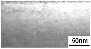
The sheet resistivity of undoped GaN without was 350 ohm/cm2. After implantation, the sheet resistivity was reduced to 25 ohm/cm2. Furthermore, the contact resistivity between the electrode materials and the GaN surface was measured. The n-type ohmic electrode material was Al/Ti/Au (30nm/100nm/50nm). Before ion implantation, the contact resistivity of the undoped GaN was 3×10⁻³ ohmcm2. After Si-ion implantation, the contact was 7×10⁻⁶ ohmcm2 as shown in Figure 1. That is, it was confirmed that Si-ion implantation into the GaN layer was very effective for reducing the contact resistivity. Furthermore the cross-seat ion of Si-implanted GaN was observed by transmission electron microscopy (TEM). Figure 2 shows a TEM image of Si-implanted GaN after annealing at 1123 K. No damage based on Si-ion implantation was observed. Therefore, it was thus confirmed that Si-ion implantation is very effective for the contact resistivity.

Figure 1. Contact resistivities versus GaN carrier concentrations.

Figure 2. Cross-sectional TEM image of GaN after Si-ion implantation and annealing at 1123 K.
GaN Mesfet
The GaN MESFET structure is as follows [Reference Yoshida and Suzuki14]. A 50 nm-thick GaN buffer layer was grown on a sapphire substrate. An undoped 1000 nm-thick GaN layer was grown on an GaN buffer layer and an AlN layer was grown on the undoped GaN layer to isolate the active layer. Lastly, a 350 nm-thick Si-doped GaN active layer was grown on the AlN layer. The surface morphology of the grown GaN was smooth. The active layer had a carrier concentration of 3×1017 cm−3 and a mobility of 250 cm2/Vsec at room temperature. Etching of the GaN was carried out by a dry-etching technique using an ECR plasma to form the FET. The etching gas was a mixture of CH4 (5 sccm), Ar (7 sccm), and H2 (15 sccm) [Reference Yoshida and Suzuki10]. The etching rate of the Si-doped and undoped GaN layers was 14 nm/min. We formed a source and drain using Au/Ti/Al, and a Schottky-gate as Au/Pt on a patterned GaN sample using an ECR sputter-evaporation method, respectively. The gate length of the GaN MESFET was 2.5 µm and the gate width was 100 µm.
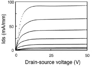
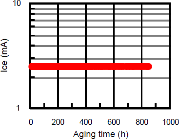
The FET property was obtained at room temperature. The breakdown voltage between gate-source was also about 80 V. The pinch-off voltage was about -8 V. The transconductanse (gm) was about 25 mS/mm. Furthermore, to investigate the high-temperature reliability of a GaN MESFET, we carried out a life test of a FET by continuous current-injection at 673 K. The FET property at 673 K was measured by continuously injecting a current of Ids at Vds=20 V and Vgs=0 V. Figure 3 shows the aging time versus Ids of GaN MESFET at 673 K. It should be noted that no change of Ids was observed for over 1010 h. The gm was also constant at 25 mS/mm. Figure 4 shows the characteristics of Ids as a function of Vds for increasing values of the gate-source voltage (Vgs) at 673 K. The pinch-off voltage was also about -8 V. The FET property was almost the same as that at room temperature, and good performance of the FET was maintained at 673 K. Using transmission electron microscopy (TEM), we also observed that the interfaces of the electrode materials and the GaN layer were not degraded.

Figure 3. Aging property of Ids of a GaN MESFET during continuous-current injection at 673 K.

Figure 4. Current-voltage characteristics (Ids-Vds) of a GaN MESFET at 673 K. The gate voltages (Vgs) was changed from 0 V to −5 V in steps of −1 V.
Based on these results, the high-temperature reliability of a GaN MESFET was confirmed, since the electrode materials did not diffuse into the GaN, and the GaN layer was not deformed at 673 K.
GaN bipolar junction transistor
We investigated the reliability of a GaN bipolar junction transistor (BJT) at high temperature. The structure of the bipolar junction transistor using GaN is shown in Figure 5 The thicknesses of the emitter, base, and collector layers were 450 nm, 350 nm, and 500 nm, respectively. The carrier concentration of the emitter and collector was 5×1017 cm−3 and the base carrier concentration was 1.5×1017 cm−3. The structure was also formed by ECR plasma etching using CH3/Ar/H2. The emitter size was 350×400 µ m2. The sizes of the base and collector were 200×150 µm2 and 450×600 µ m2, respectively. The electrode materials of the emitter and collector were formed using Au/Ti/Al. The base contact was also formed using Au/Ti/Ni.

Figure 5. Schematic drawing of the structure of an n-p-n bipolar junction transistor using a GaN.
In order to investigate the operation of the bipolar junction transistor at 573 K, the current-voltage characteristics, as measured in the common emitter mode at 573 K, were measured. It was found that the bipolar junction transistor performance at 573 K remained unchanged, as shown in Figure 6, although Ic was slightly changed compared with that produced at room temperature. The current gain (dIc/dIb) was about 10. Figure 7 shows the p-n junction property between the base and the emitter electrodes during heating at 573 K. The breakdown voltage was over 10 V. Furthermore, a life test of a bipolar junction transistor was carried out. Figure 8 shows the result of an aging test at 573 K. Here, Vc was 4 V and Ib was 120 µA. Ic did not change for over 850 h. That is, it was confirmed that the bipolar junction transistor was operated for over 850 h. It was also found by SIMS that interfaces between the electrode materials and the GaN layer after heating at 573 K was abrupt and that the GaN was not affected by heating at 573 K. We thus confirmed the reliability of the GaN bipolar junction transistor at 573 K.

Figure 6. Current (Ic) - voltage (Vc) characteristics as measured in the common-emitter mode at 573 K. The base current (Ib) was changed from 20 µA in steps of 50 µA.

Figure 7. p-n junction property between of the base and emitter electrodes at 573 K.

Figure 8. Aging property of GaN BJT at 573 K.
Conclusion
A high-quality GaN was grown using GSMBE. A GaN MESFET and an n-p-n bipolar junction transistor were fabricated. The life test of a GaN MESFET at 673 K was examined by continuous current-injection at 673 K. We confirmed that the FET performance did not change at 673 K for over 1010 h. No degradation of the metal-semiconductor interface was observed by SIMS or TEM. Furthermore, the fabrication of a GaN bipolar junction transistor was carried out. The life performance of the bipolar transistor at 573 K was examined during continuous current-injection at 573 K. We confirmed that the performance of the bipolar transistor did not change at 573 K for over 850 h. No degradation of the metal-semiconductor interface was observed by SIMS or TEM. The reliability of a GaN BJT at high temperature was thus confirmed.