Introduction
In the past few years nitride-based nanostructures have been successfully used in the fabrication of optoelectronic devices as well as in the development of high frequency and high-temperature electronic devices [Reference Nakamura and Fasol1-Reference Smorchkova, Elsass, Ibbetson, Vetury, Heying, Fini, Haus, DenBaars, Speck and Mishra4]. Most of the applications made so far are based on the hexagonal (h) phase of the nitride materials. However, cubic (c) GaN/GaAs (001) layers grown by metal organic chemical vapor deposition (MOCVD) and by plasma assisted molecular beam epitaxy (MBE) have recently been used to fabricate p-n junction light emitting diodes [Reference Yang, Zheng, Li, Wang, Xu, Wang, Hu and Han5-Reference As, Richter, Busch, Lübbers, Mimkes and Lischka6]. In order to improve on the performance of these devices, further studies of the optical and electrical properties of the nitride layers are required. Particularly, the improvement of the n- and p-type doping levels and carrier mobilities in these layers is a crucial task for the device technology, mainly for that involving the cubic phase of the materials [Reference Teles, Scolfaro, Leite, Ramos, Tabata, Castineira and As7,Reference As, Schikora, Greiner, Lübbers, Mimkes and Lischka8].
In the present work measurements of carrier concentrations and mobilities of unintentionally doped c-InN and c-GaN MBE grown epitaxial layers are performed as a function of temperature. c-GaN samples doped with silicon are also investigated in the temperatures range 10 to 350K. The carrier concentrations and mobilities obtained for the cubic (zinc-blend) InN and GaN layers are compared with the results available for the corresponding hexagonal (wurtzite) nitride samples.
Samples
The c-InN sample was grown on GaAs/InAs buffer layers firstly grown on GaAs (001) substrate by plasma-assisted MBE. We have used a Riber 32-system equipped with elemental sources of Ga, As, In, Si and an Oxford Research CARS25 radio frequency plasma source for the reactive nitrogen. After the growth of the GaAs buffer layer at a temperature of 610°C, we grew a 300nm layer of InAs at a temperature of 480°C under (2×4) reconstruction. The growth of the InN layer, with about 300nm width, was performed at a reduced temperature of 450°C. Further details about the growth of the c-InN layer are given in Refs. [Reference Lima, Tabata, Leite, Kaiser, Schikora, Schöttker, Frey, As and Lischka9,Reference Tabata, Lima, Teles, Scolfaro, Leite, Lemos, Schöttker, Frey, Schikora and Lischka10]. The same Riber 32-system was used to grow the intrinsic and the Si-doped c-GaN layers on GaAs (001) substrates. Elemental Si was evaporated at source temperatures between 750°C and 1100°C.
The widths of the c-GaN layers are of about 0.8 μm [Reference As, Schikora, Greiner, Lübbers, Mimkes and Lischka8,Reference As, Richter, Busch, Schöttker, Lübbers, Mimkes, Schikora, Lischka, Kriegseis, Burkhardt and Meyer11]. To perform the electrical characterization of the samples we have used Hall-effect measurements as a function of temperature at a 0.5T magnetic field. Ohmic contacts using In were accomplished according to Van der Pauw geometry. The characteristics of our samples are shown in Table I.
Table I – Characteristics of the cubic nitride samples: ND is the nominal silicon concentration, n and p are the measured electron and hole concentrations at300K, respectively.

Intrinsic c-InN
The measured carrier concentration in the unintentionally doped c-InN layer as a function of inverse temperature is shown in Fig.1. High-electron concentrations of the order of 1020 cm−3 were found in the range of temperature from 10 to 300K. This metallic behavior was also observed in MOCVD grown h-InN layers and attributed to the presence of native nitrogen vacancies in the sample [Reference Miura, Ishii, Yamada, Konagai, Yamauchi and Yamamoto12]. The same behavior was also observed for metal organic MBE grown c-InN [Reference Geerts, Mackenzie, Abernathy, Pearton and Schmiedel13]. Fig. 1 shows that a sharp increase of the electron concentration occurs when the temperature raises above 200K. This behavior which was not observed in the h-InN layers may indicate that another deeper donor level, with activation energy of about 94,5 meV, exists in our c-InN layer. It is well known that ab initio calculation lead to zero or negative gap values for the InN binary compound. This fact has hindered severely our knowledge about native defects in this material from theory. On the other hand, very few attempts have been made so far to grow c-InN films [Reference Lima, Tabata, Leite, Kaiser, Schikora, Schöttker, Frey, As and Lischka9]. Thus, systematic effort is required to identify the origin of the defects or impurities, which give rise to such high electron concentrations observed in our c-InN layer.

Figure 1: Electron concentration as a function of temperature for the intrinsic c-InN. The dashed line is used to calculate the activation energy ED=94.5 meV.
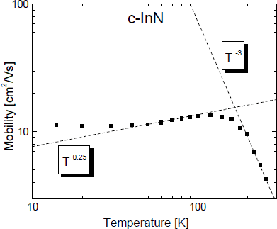
The electron mobilities measured by us in the c-InN layer as a function of temperature are shown in Fig.2. In the temperature range of 10 to 260K the measured mobilities are one order of magnitude smaller than those observed for the h-InN films [Reference Miura, Ishii, Yamada, Konagai, Yamauchi and Yamamoto12]. This probably indicates the best quality of the hexagonal films. Above 200K a decrease of the mobilities follows the sharp increase in the concentrations. Attempts were made to adjust the observed behavior of the mobilities to different scattering and screening mechanisms. We expect that impurity scattering is involved in the changes of the mobility at lower temperatures and scattering by phonons is active at higher temperature, although the T dependencies obtained by us deviate from the expected ones for these mechanisms. Further investigations of both, h-InN and c-InN films are required to understand and control their electrical properties.

Figure 2: Mobility as a function of temperature for the intrinsic c-InN.
Intrinsic c-GaN
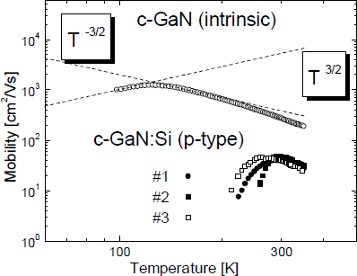
The Hall carrier concentration measured as a function of temperature for the nominally undoped c-GaN sample is shown in Fig. 3. Due to the presence of an intrinsic acceptor level a background hole concentration is obtained. This concentration increases from p=3.7 × 1013 cm−3 at 100 K (not shown in the Figure) to p=2.0 × 1016 cm−3 for T=350 K. The carrier concentration behavior near the room temperature region allows us to determine an activation energy of EA=166 meV for the involved acceptor. Therefore, we can estimate an acceptor concentration of NA ≈ 4 × 1018 cm−3 for this nominally undoped sample. The measured hole mobility is presented in Fig. 4 as a function of temperature. The mobility initially increases with temperature reaching a maximum value of 1250 cm2/Vs at T=120 K and then decreases to a value of 283 cm2/Vs at room temperature. As can be seen in Fig. 4, the T3/2 behavior, shown at low temperature, suggest that in this region the mobility is limited by ionized impurity scattering. Above 120 K the decrease of mobility, proportional to T−3/2, is probably due to phonon scattering.

Figure 3: Hole concentration as a function of temperature for the intrinsic c-GaN. The dashed line is used to calculate the activation energy EA=166 meV

Figure 4: Mobility as a function of temperature for the intrinsic c-GaN (opened circle) and for the lightly doped c-GaN:Si (closed circles, closed squares, and opened squares).
Lightly Doped c-GaN:Si
We expect to obtain n-type conductivity for c-GaN when it is doped with Si. Contrary to that, p-type conductivity is measured for samples with a Si concentration below 1.2 × 1019 cm−3. This is due to the fact that the acceptor background, present in intrinsic c-GaN, is not yet completely compensated for these concentrations. The hole concentrations measured for the samples #1, #2, and #3 are shown in Fig. 5. They all present the same behavior as a function of temperature, i.e., a decreasing of concentration as the temperature is lowered passing by a minimum and then increasing again when the temperature is further decreased. From the decrease of the concentration in the region near the room temperature an activation energy can be calculated yielding the values of 157, 154, and 171 meV for the samples #1, #2, and #3, respectively. All these values are very close to the activation energy measured for the acceptor level of the intrinsic c-GaN. This allows us to infer that the same acceptor level provides the measured high temperature hole concentrations in these samples. The increase of concentration at low temperature is probably due to a frozen of the carriers into a localized level. The shape of the mobility measured as a function of temperature (Fig. 4) is very similar to that presented by the intrinsic c-GaN. Nonetheless, the mobilities are much smaller and the T3/2 (low temperature) and T−3/2 (high temperature) dependence cannot describe their behavior anymore. This indicates that besides the scattering mechanisms described above, other mechanisms are involved.

Figure 5: Hole concentration as a function of temperature for the lightly doped c-GaN:Si. The dashed lines are used to determine the activation energies.
Heavily Doped c-GaN:Si
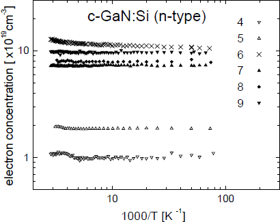
When the Si concentrations in c-GaN are higher than 2.5 × 1019 cm−3 a n-type conductivity is obtained. For these concentrations the acceptor level is completely compensated and we have a degenerated semiconductor. The electron concentration as a function of temperature measured for samples #4 to #9 is shown in Fig. 6. A metallic behavior can be observed, since the electron concentration does not change as the temperature is varied, which is typical of highly degenerated semiconductors.

Figure 6: Electron concentration as a function of temperature for heavily doped c-GaN:Si.
Conclusions
Cubic InN and GaN binary semiconductor compounds were investigated by Hall effect measurements as a function of temperature. The InN sample shows a very high electron concentration (n≅1020cm−3). At temperatures above 200K, a donor with an activation energy of ED=94,5 meV leads to a sharp increase of the electron concentration. The mobility at low temperature increases with T1/4 while a decrease with T−3 is observed at a high temperature region. Nominally undoped c-GaN shows a p-type background concentration which varies from 1013 to 1016 cm−3 as the temperature is raised. The mobility dependence on temperature suggests that dislocations and ionized impurities are the scattering mechanisms at low temperature (T3/2), while phonon scattering is the dominant one at a high temperature (T−3/2). Si-doped c-GaN has p-type conductivity for Si-doping concentration below ND≅1.2×1019cm−3, and is highly n-type degenerated for ND≥1.2×1019cm−3. The behavior of the mobility as a function of temperature for the p-type c-GaN:Si is similar to that observed for the undoped sample, but its behavior is no longer described by T3/2 and T−3/2, indicating that other scattering mechanisms like dislocation scattering are taking place in our samples.
Ackowledgements
This work was performed with partial support of a “CAPES/DAAD/PROBRAL” project within the Brazil/Germany scientific collaboration program. The authors also acknowledge financial support from FAPESP (Brazilian funding agency) and DFG (Deutsche Forschungsgemeinschaft).