

Carbon, with its abundance and high solid solubility, has been pursued extensively as a dopant for semiconducting metal dichalcogenides. Previously reported carbon-doping methods produce mixtures of doped materials and metal carbides instead of pure doped materials, due to the high doping temperatures needed (e.g., 800°C). Now a research team led by Mauricio Terrones, Susan B. Sinnott, and Saptarshi Das from The Pennsylvania State University has developed a mild means to introduce carbon atoms into WS2 monolayers.
The researchers used a plasma-enhanced chemical vapor deposition (PECVD) system to dope the WS2 sheets with hydrocarbon groups at 400°C, roughly half the required temperatures of conventional methods. Because of the low temperature and short duration (15 min), the product consisted exclusively of carbon-doped WS2. This technique was published in a recent issue of Science Advances (doi:10.1126/sciadv.aav5003).
According to Terrones, one of the corresponding authors of this work, the team’s goal was “to study the transformation of a chalcogenide to a carbide, and doping metal chalcogenides with carbon was the first step.” Unlike traditional strategies requiring high-temperature annealing to generate reactive species for doping, the PECVD system created carbon dopants using plasma with a radio frequency of 13.56 Hz at 400°C. The reactive plasma decomposed methane gas into carbon and hydrocarbon radicals. When these species diffused to the intrinsic sulfur vacancies of WS2, they embedded themselves into the crystal lattice of WS2 by forming covalent bonds with the neighboring tungsten atoms, forming carbon-doped WS2.
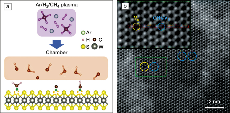
(a) A schematic illustration of the plasma-enhanced chemical vapor deposition system. (b) Aberration-corrected scanning transmission electron microscope image showing one sulfur vacancy (yellow circle) and three CH-doped sites (blue circles). Credit: Science Advances.
The carbon dopants modified the optical and electronic properties of the single-layer WS2. Density functional theory simulations and aberration-corrected high-resolution transmission electron microscopy studies unveiled that the dopants were CH groups. These incorporated groups decreased the bandgap of the single-layer WS2, which red-shifted the photoluminescence peak by 0.15 eV. Additionally, when the carbon-dopant concentration progressively increased from zero to 3.3 at.%, the electronic nature of the WS2 monolayers transitioned from n-type to p-type.
Jin Z. Zhang, a professor in the Department of Chemistry, University of California, Santa Cruz, highlights the multiple-atom doping feature of this work. “Most doping in semiconductors involves the use of single atoms or ions,” says Zhang. “This work is unique in that it demonstrates the successful doping of carbon-hydrogen groups, besides single carbon atoms, within sulfur monovacancies of WS2 using a novel plasma-assisted approach.”
The researchers are extending the PECVD technique to “understanding the effects of other dopants in transition-metal dichalcogenides,” Terrones says. Additionally, they are exploring ways to prepare metal oxide semiconductors with gradient doping schemes. Such tailor-made semiconductors can function as high-performance complementary metal oxide semiconductors in integrated circuits.
