Introduction
Living in the information age we are surrounded by technology that enables us to solve problems on a daily basis, which were thought to be intangible just a couple of decades ago. High-performance computation, ubiquitous communication as well as instant storage of large sets of data have allowed information technology to transform virtually all aspects of our lives and has changed society in an irrevocable way: computer-aided design strategies to develop new products, realistic simulations to predict and verify their functionalities, control of robotic manufacturing processes, and the role of computers to orchestrate complex processes, such as managing supply chains in industry or large-scale science experiments. Furthermore, new social media have emerged and videoconferencing platforms enable fast, high quality, personal interaction in affordable ways. Similarly, cloud computing allows sharing large data sets and provides concurrent access from all over the world in real time. All these examples attest to the ways in which information technology has revolutionized how we construct, build, communicate, and understand our world.
Without any doubt, semiconductor materials in general, and silicon in particular, constitute the material basis for all these opportunities. In semiconductors, two key functionalities are ideally met—(1) modulating the flow of charge carriers by an applied electric field thereby enabling manipulation, amplification, and storage of electrical signals; and (2) transducing electrical signals into optical signals and vice versa at very fast time scales. Improved synthesis and fabrication technologies of these materials, the development of nanoscale metrology tools, and consequent exploitation of computers to simulate devices and understanding materials from first-principles have formed a self-feeding cycle of innovation and technology advancements. This enables the continuous improvement of device performance, faster operation, and increased level of integration density at lower costs that is witnessed today. But, how long will this process continue and what will come next?
Gordon Moore's prediction[ Reference Moore 1 ] to double the number of transistors every 2 years has held for the past four decades with a near million-fold increase in transistor density. In the mid-2000s, single-thread microprocessor clock speed stagnated to limit heat dissipation, which marked the end of classical scaling and the introduction of power-constraint scaling.[ Reference Koomey and Naffziger 2 ] Multi-core architectures have been used to continue enhancing computing performance per chip keeping the projected pace. At present, however, continued scaling has slowed down to a 3-year turnaround. It is anticipated that the 10 nm technology node will be introduced in 2017, while the 7 nm node is projected for 2020, owed to the ever increased complexity of the chip manufacturing process.[ Reference Cross 3 ] The slowing cadence of Moore's Law signals that profitability of advancements are becoming smaller, thus favoring a strategy to look for new material opportunities to augment the current hardware and expand beyond the current complimentary metal–oxide–semiconductor (CMOS) technology. With silicon being the material of the 20th century, emerging electronic materials of the 21st century will add novel functionalities not feasible in conventional semiconductors, thereby permitting higher throughput and more energy-efficient hardware solutions for computation, communication, and data storage.
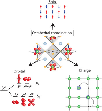
Transition metal oxides (TMOs) represent such a class of materials. While the rationale for honing in on Si and other semiconductors was their electronic response to external electric field, robustness, ease of surface passivation, and excellent electronic transport properties at room temperature, the conduction bands in TMOs are derived from d-orbitals stemming from the transition metal element, which provide additional functional complexity if partially filled. As graphically depicted in Fig. 1, electrons in a solid have three fundamental properties: charge, spin, and orbital degrees of freedom (DOF). In conventional semiconductors, the completely filled bands quench the spin and orbital DOF, which in turn do not play any role, leaving charge modulation via field effect as the primary control mechanism. In contrast, in TMOs the spin and orbital DOF are active and coupled, which can give rise to frustration resulting in a manifold of competing ground states with different order phenomena, and, therefore, coupled phase transitions. For example, the proximity to the fluctuating anti-ferromagnetic phase is thought to be key for the stabilization of the high-temperature (high-T C) superconducting state in the complex cuprate superconductors.[ Reference Lee and Wen 4 ] Furthermore, cross-coupling of magnetic and orbital order can drive field-dependent metal–insulator transitions (MITs) that give rise to colossal magnetoresistive effects in manganites.[ Reference Tokura and Tomioka 5 ] TMOs have widely been the focus of fundamental research, with extensive emphasis placed on peculiar properties of the manganites (A, A′)MnO3 where A and A′ are, respectively, rare-earth and alkali-earth cations, nickelates (A, A′)NiO3, and the chemically more complicated layered cuprates (for example, HgBa2Ca2Cu3O8, with the highest T C of 134 K[ Reference Schilling, Cantoni, Guo and Ott 6 ]).[ Reference Heber 7 – Reference Tokura 9 ]

Figure 1. Octahedral coordination of the vanadium cation as the fundamental building block of properties in all vanadium oxide phases. The strong electron correlation effects couple the three electron DOF, spin, orbital, and charge; which can result in frustration and competing ground states with different long-range order, electronic and optical properties that give rise to the wide range of properties observed in vanadium oxide compounds.
In contrast to these TMOs containing middle- and late-transition-metal elements, vanadium-based (V-based) oxides have been far less studied. The close proximity of electronic phases with disparate electronic properties observed in V-based oxides makes them attractive as electronic phase change materials (PCMs). Unlike in the case of semiconductors, which have been perfected over decades to the highest level of maturity, we are only at the beginning to learn how to stabilize and control these electronic phases and how to put them to use in practical devices. Here, we review recent advances and project future opportunities that V-based TMO materials possess. We focus on binary and ternary V-based oxides, which show a wide range of ground states ranging from metals to insulators, coupled charge-, spin-, and orbital-ordered phases, to superconductors (see Refs. Reference Tokura9–Reference Yamauchi, Isobe and Ueda13 and reference therein). The outline is as follows: In the section “Strong electron correlations in V-based oxides”, the physical concepts underpinning the understanding of electronic properties in V-based oxides are outlined and how these drastically differ from semiconductor materials. In the section “MIT transition in binary vanadium compounds: VO2 and V2O3” the challenges to synthesize specific binary vanadium oxides (V x O y ) is discussed and how better control over the deposition has recently enabled progress in the quality of ultrathin VO2 films. Three specific examples are reviewed how the electronic PCM VO2 has recently been applied to create practical electronic devices with competitive functionality (1) by augmenting metal–oxide–semiconductor field effect transistors (MOSFET), enabling a positive feedback in the turn-on characteristic to surpass the Boltzmann limit of 60 mV/decade (section “Augmenting field effect transistors (FETs) with VO2”); (2) to serve as a scalable hardware platform to enable non-Boolean computing schemes via synchronization behavior through capacitively coupled charge oscillator devices stabilized in their phase coexistence regime (Section “Non-Boolean computing using charge coupled VO2 oscillators”); and (3) as an electronic switch, uniquely balancing the high operation frequency of microelectromechanical systems (MEMS) switches with the reliability and fast switching characteristics of a transistor-based solid-state radio frequency (RF) switch (section “VO2 as RF switch”). In the section “Ternary oxide vanadates”, the discussion is expanded toward ternary vanadium oxide phases. Starting by exemplifying the strong electron correlation effects in SrVO3 and CaVO3 in the section “Ternary oxide vanadates”. A the challenges in growing thin films and how recent advances have made strides to simplify the growth procedure while improving material quality is reviewed in Section (Thin-film growth of AVO3 perovskites). As discussed in the section “A route to enhanced correlation effects: thickness-driven MIT” thin-film epitaxy can be used as a route to enhance correlation effects through dimensional confinement to drive the strongly correlated metal SrVO3 into an insulating phase. Then, as a direct application of the electron-correlation physics, section “Correlated metals as TCs” discusses how the specific band structure of vanadates and pronounced electron interaction effects inherent to the correlated metals SrVO3 and CaVO3 offer a novel design strategy to strike a better balance in the mutually exclusive properties of optical transparency and electrical conductivity, thus constituting a new paradigm in field of transparent conducting thin films. In section “The Mott-insulating phase in rare-earth vanadates”, opportunities in the rare-earth perovskites (RVO3) centered on the strongly spin–orbital coupled, Mott-insulating ground state for photovoltaic applications are reviewed. We finally close with an outlook about future vanadium oxide materials and their prospects for their application into the next generation of optoelectronic devices.
Strong electron correlations in V-based oxides
The atomic scale interactions that determine the macroscale electronic properties of a solid are complex. Deriving a solution for the many-body wave function of allowed electronic states that considers the Coulomb interaction between electrons and ions constituting the crystalline lattice, but also the repulsive interaction among all electrons, is impossible. For a large number of materials satisfactory predictions of electronic properties, however, can be obtained by employing the Hartree–Fock formalism (see, e.g., Ref. Reference Ashcroft and Mermin14) where all many-body interactions except the electron–electron interaction are incorporated. The ground state is then described by a wave function of single, non-interacting quasi-particles (herein, unless otherwise stated electrons will refer to quasi-particles) that are considered nearly free and independent, i.e., not correlated, and can be computed self-consistently. The interactions with the periodic arrangement of ions forming the crystal are entirely accrued into a rescaled quasi-particle mass m b *—the electron effective mass in the respective band b. For semiconductors, where the conduction and valence band are derived from s- and p-like orbitals, this nearly-free-electron picture provides an accurate description. This is made possible by the large kinetic energy of the carriers ħ 2 k 2/(2m b *), with ℏ being the reduced Planck constant and k the electron wavevector that is of the order of the inverse lattice parameter, relative to the repulsive Coulomb interaction energy among the electrons. In conventional semiconductors, the kinetic energy is of the order of 10–20 eV[ Reference Cardona and Pollak 15 ] due to small electron effective mass that is typically one-tenth that of an free-electron mass. The electron–electron interaction, the potential energy of two electrons getting into very close proximity, i.e., being at the same lattice site, is much smaller, ~1–2 eV[ Reference Fujimori, Yoshida, Okazaki, Tsujioka, Kobayashi, Mizokawa, Onoda, Katsufuji, Taguchi and Tokura 16 ] and can therefore be neglected. In this case, electrons barely affect each other, they are nearly free and their motion is not correlated.
In contrast, for many TMOs, including vanadium oxide phases, the approximation of the many-particle problem using the picture of nearly free electrons is found to not adequately describe real materials. Here, the kinetic energy and the Coulomb potential energy that arises from electron–electron interactions are of similar magnitude. The conduction and valence bands in conventional semiconductors stem from s- and p-hybridized orbitals, which have significant overlap giving rise to a large band width, sizeable band dispersion, and, thus a small effective mass and large kinetic energies; in contrast, the localized 3d orbitals in TMOs form the partially occupied conduction band. The far more spatially localized and more directional shape of 3d orbitals cause a much smaller orbital overlap, and thus smaller band width W and larger effective masses that are similar to or even larger than the mass of the free electron in vacuum. A one order of magnitude increase in the free-electron mass directly reduces the electron's kinetic energy in the TMO d-bands making it comparable with the Coulomb repulsion, thus rendering the simple non-interacting picture invalid.
To illustrate how electron correlation effects modify the underlying physics, Fig. 2 schematically shows a comparison of the optical conductivity σ(E) [Fig. 2(a)], the band structure with conduction band width W and band gap E g , i.e., the energy momentum relation E(k) of electrons, along with the associated density of states, DOS [Fig. 2(b)]. In addition, the spectral function of the electrons A(k, ω) is shown as well [Fig. 2(c)], which represents the distribution of an ensemble of electrons having momentum k and energy E = ℏω. We first consider the optical conductivity. In general, photoexcitation causes a complex response of the many-body ground state; however, for uncorrelated materials, i.e., materials that have a negligible electron–electron interaction expressed by a vanishing Coulomb potential (U = 0), these excitations can be understood using the concept of non-interacting quasi-particles. For band insulators, the lowest possible excitation is to promote single electrons from filled states in the valence band (blue), to unoccupied states in the conduction band (white). The interband transition appears as the red shaded peak in σ(E). For the case of a conventional metal with uncorrelated electrons, where the Fermi level E F intersects the conduction band, lower-energy excitations are possible, because transitions from occupied to unoccupied states are possible within the same band. These intraband transitions with small excitation energies appear as the low-energy Drude peak (shaded yellow) in the optical conductivity. For these materials with negligible correlation effects, represented by a vanishing electron–electron interaction potential U, the respective spectral function shown in Fig. 2(c) is simply A(k, ω) ~ δ[ω − E(k)]. It implies that electrons are described by orthogonal single-particle eigenstates with infinite lifetimes, and can be distinguished by wavevector k, the main quantum number, which is associated with a specific energy E. This single-valued relation, the dispersion relation E = ℏ2 k 2/(2m b *), is a direct result that electrons only interact with the periodic lattice potential.

Figure 2. Comparison of various properties for systems without electron correlation effects (left) and strong electron correlated (right): (a) optical conductivity σ(E), (b) the band structure ε(k) and density of states DOS, (c) the spectral function A(k, ω). Dashed and solid curves in (b) represent inter- and intraband transitions, giving rise to a peak (red) and the Drude tail (yellow) in the optical conductivity. Solid and dashed arrows in (c) illustrate the changes in the spectral function A(k, ω) with increasing correlation strength, causing reduction and widening (Δ ~ Z k −1) of the coherent peak at ω = 0 and a spectral weight transfer to the incoherent side peaks, respectively.
The addition of an electron–electron interaction breaks the ideal periodicity of the underlying lattice, thus requiring a modified framework to properly account for experimental observations. As electron correlation becomes sizeable (U > 0) additional features in the optical conductivity appear. As shown on the right side of Fig. 2(a), the magnitude of the Drude peak at low energy decreases and a new peak, shaded pink, at higher energy appears for U < W. This change is reflected in the DOS as well where lobes emerge at the conduction band edges and the magnitude at the Fermi energy is diminished. Electrons are now correlated, which implies that their energies now also depend on the spatial arrangement of adjacent electrons in the near vicinity. Even being in the same state, represented by wavevector k, they can be in different local configurations and thus at different energies, which is captured by a more complex spectral function A(k, ω) shown in Fig. 2(c). Note that the magnitude of the coherent peak in the spectral function of the electron, representing delocalized, free moving quasi-particles, is renormalized and broadened by the factor Z k . Additionally, incoherent side peaks emerge at E = ± U/2 relative to the coherent peak. Electrons in correlated systems can have a range of energies with a span of the Columbic interaction energy U, because despite a very well-determined momentum defining the kinetic energy it can be in different local electron arrangements, ranging from virtually no other electrons in its spatial vicinity energy, to experiencing the maximum Coulomb effect U from the electron–election interaction. The local nature breaks the periodic potential that makes the band structure well defined, and the dispersion relation becomes smeared, schematically illustrated in Fig. 2(b).
The correlation effects can be captured by renormalizing the band mass m b * by m* = m b */Z k , which reduces the kinetic energy, the band width W and thus the itinerant character of electrons compared with results obtained in the Hartree–Fock approximation. The band dispersion is not a single-valued function anymore, where for each wavevector k only a very specific energy value is found. Instead it can be considered as convolution of the spectral function with the band structure to account for the distribution of different local electron configurations. This is in dramatic difference to conventional materials with negligible electron–electron interaction. In the presence of sizeable electron correlation, the band structure also depends on the spatial arrangement of the electrons. Therefore band structure can be potentially altered in response to changes of the spatial arrangement of electrons.
Further increasing electron correlation strength, represented by U, electrons are becoming less itinerant and more become localized, which is captured by a further spectral weight transfer from the coherent to incoherent part in A(k, ω), a reduced life time and magnitude of the itinerant quasi-particle (0 < Z k < 1). In the extreme limit of electron correlation, U > W and Z k = 0 and the coherent peak in A(k, ω) vanishes and hence the quasi-particle effective mass of itinerant electrons diverges and their lifetime approaches zero: they no longer exist. Only the incoherent peaks remain forming the lower and upper Hubbard band separated by the Mott gap E M. While the lower, fully occupied Hubbard band represents the singly occupied crystal site, the upper, unoccupied Hubbard band represents the doubly occupied site, and, therefore the energy separation is proportional to the Coulomb energy U of interacting electrons.
This correlation-induced transition from a metallic phase to an insulating ground state, as proposed by N. F. Mott, is the underlying physics of the early transition metal oxides.[ Reference Mott and Friedman 17 , Reference Zaanen, Sawatzky and Allen 18 ] While TMOs with partially filled d-bands are expected to be metallic from simple band structure arguments, electrons are being localized due to the strong electron–electron interaction and hence do not contribute to conduction making the material electrically insulating. The Mott transition is directly tied to the local bonding environment by the electron interaction strength U and orbital overlap determining the band width W. Therefore, the bonding environment is key to understand and control the ground state. While the valence state of vanadium can range from 2+–5+ the associated ionic radii only allow for sixfold coordination when bonded to oxygen according to Pauling's rules[ Reference Pauling 19 ]. In case of vanadium, it therefore takes the shape of an oxygen octahedron with V located inside, as shown in the center of Fig. 1. This forms the fundamental building block of virtually all V-based oxide materials, mediating the complex coupling between the competing charge, spin, and orbital DOF.
MIT in binary vanadium compounds: VO2 and V2O3
Among the materials exhibiting MITs, perhaps the most intensely studied compounds are the binary oxides of vanadium.[ Reference Imada, Fujimori and Tokura 10 , Reference Morin 20 ] In particular, V2O3, the trivalent oxide of vanadium, exhibits a well-studied MIT from a high-temperature paramagnetic metallic (PM) to a low-temperature AFI (antiferromagnetic insulating) state at 154 K, along with a change in electrical conductivity by eight orders of magnitude.[ Reference Feinleib and Paul 21 ] Similarly an MIT occurs in the tetravalent compound VO2 at 340 K, but in contrast to V2O3 it transitions from a high-temperature PM state to a low-temperature, PI (paramagnetic insulator state), exhibiting five orders of magnitude change in conductivity.[ Reference Ladd and Paul 22 ] Symmetry-lowering structural distortions accompany the MITs of V2O3 and VO2 making them a first-order transition. Despite extensive investigations since the first observations of this phenomena dating back more than half a century, the exact mechanisms and intricate interplays of the different DOF driving the MITs are still controversially discussed, while structure and electronic properties have been characterized in detail are comprehensively understood.[ Reference Imada, Fujimori and Tokura 10 , Reference Hansmann, Toschi, Sangiovanni, Saha-Dasgupta, Lupi, Marsi and Held 23 , Reference Qazilbash, Schafgans, Burch, Yun, Chae, Kim, Kim and Basov 24 ]
V2O3 in the high-temperature metallic state crystallizes into the corundum structure (space group $R\bar 3c$
); see Fig. 3(a). Vanadium is displaced out of the center of the oxygen octahedra away from the nearest neighboring vanadium.[
Reference Morin
20
] The crystal field splits the V 3d orbitals into the high-energy, doubly degenerate
$R\bar 3c$
); see Fig. 3(a). Vanadium is displaced out of the center of the oxygen octahedra away from the nearest neighboring vanadium.[
Reference Morin
20
] The crystal field splits the V 3d orbitals into the high-energy, doubly degenerate $e_g^\sigma $
states and the low-energy, triply degenerate t
2g
states, the latter occupied by both valence electrons with a total spin S = 1 per V3+
lattice site.[
Reference Qazilbash, Schafgans, Burch, Yun, Chae, Kim, Kim and Basov
24
] The degeneracy of the partially filled t
2g
states is lifted due to a trigonal distortion of the octahedron, which then split into a high-energy, non-degenerate a
1g
state and two low-energy, doubly degenerate
$e_g^\sigma $
states and the low-energy, triply degenerate t
2g
states, the latter occupied by both valence electrons with a total spin S = 1 per V3+
lattice site.[
Reference Qazilbash, Schafgans, Burch, Yun, Chae, Kim, Kim and Basov
24
] The degeneracy of the partially filled t
2g
states is lifted due to a trigonal distortion of the octahedron, which then split into a high-energy, non-degenerate a
1g
state and two low-energy, doubly degenerate $e_g^\pi $
states. While the derived a
1g
band would be nominally empty, the lower lying
$e_g^\pi $
states. While the derived a
1g
band would be nominally empty, the lower lying $e_g^\pi $
band would be half-filled; however, due to hybridization of both states a significant band overlap results allowing for metallic conduction.[
Reference Hansmann, Toschi, Sangiovanni, Saha-Dasgupta, Lupi, Marsi and Held
23
] Upon cooling through the transition temperature, V2O3 undergoes a structural transformation to the monoclinic (I2/a) phase; see Fig. 3(b).[
Reference Dernier and Marezio
25
] The V is displaced within the oxygen octahedra such that it forms V–V pairs through edge-sharing oxygen bonds. This dimerization is accompanied with a volume decreases by 1.3%, the c/a ratio increases by 1.4%, and the
$e_g^\pi $
band would be half-filled; however, due to hybridization of both states a significant band overlap results allowing for metallic conduction.[
Reference Hansmann, Toschi, Sangiovanni, Saha-Dasgupta, Lupi, Marsi and Held
23
] Upon cooling through the transition temperature, V2O3 undergoes a structural transformation to the monoclinic (I2/a) phase; see Fig. 3(b).[
Reference Dernier and Marezio
25
] The V is displaced within the oxygen octahedra such that it forms V–V pairs through edge-sharing oxygen bonds. This dimerization is accompanied with a volume decreases by 1.3%, the c/a ratio increases by 1.4%, and the $e_g^\pi $
band is pushed below the a
1g
band by ~0.5 eV.[
Reference Qazilbash, Schafgans, Burch, Yun, Chae, Kim, Kim and Basov
24
] The distortion increases the exchange interaction between nearest-neighbor vanadium atoms and leads to the coincident antiferromagnetic ordering of the t
2g
orbitals; however, the exact occupation of electrons within these orbitals is still not fully understood.[
Reference Qazilbash, Schafgans, Burch, Yun, Chae, Kim, Kim and Basov
24
,
Reference Chatterjee
26
–
Reference Tanaka
29
]
$e_g^\pi $
band is pushed below the a
1g
band by ~0.5 eV.[
Reference Qazilbash, Schafgans, Burch, Yun, Chae, Kim, Kim and Basov
24
] The distortion increases the exchange interaction between nearest-neighbor vanadium atoms and leads to the coincident antiferromagnetic ordering of the t
2g
orbitals; however, the exact occupation of electrons within these orbitals is still not fully understood.[
Reference Qazilbash, Schafgans, Burch, Yun, Chae, Kim, Kim and Basov
24
,
Reference Chatterjee
26
–
Reference Tanaka
29
]

Figure 3. Crystal structure (top) and energy-level diagram (bottom, adapted with permission from Ref. Reference Qazilbash, Schafgans, Burch, Yun, Chae, Kim, Kim and Basov24. Copyrighted by the American Physical Society) of V2O3 (a, b) and VO2 (c, d) in the high-temperature metal phase (a, c), and the low-temperature insulating phase (b, d). The red arrows indicate the atomic displacements across the structural transition.
Despite the large change in resistivity arising from the formation of an energy gap separating the highest occupied from the lowest unoccupied state, the MIT in V2O3 occurs at too low temperatures to be of practical relevance for applications. A transition temperature of 340 K makes VO2 more attractive for applications, similar to the less studied V3O5 phase also exhibiting an MIT above room temperature (150 °C), albeit with a much smaller change in resistivity.[
Reference Chudnovskii, Terukov and Khomskii
30
,
Reference Khoi, Simon and Eastwood
31
] VO2 is paramagnetic in its high symmetry metallic state with rutile structure (space group P42/mmm), shown in Fig. 3(c), and undergoes an MIT to the monoclinic (M1) insulating phase.[
Reference Morin
20
] Similar to V2O3, in the high-temperature metallic phase, the t
2g
orbitals are split into an a
1g
and two $e_g^\pi $
states that overlap.[
Reference Qazilbash, Schafgans, Burch, Yun, Chae, Kim, Kim and Basov
24
] As VO2 is cooled through the MIT transition the symmetry is lowered via a monoclinic distortion that is associated with V-pair formation (dimerization); see Fig. 3(d). The a
1g
band is then further split into an upper and lower part while the
$e_g^\pi $
states that overlap.[
Reference Qazilbash, Schafgans, Burch, Yun, Chae, Kim, Kim and Basov
24
] As VO2 is cooled through the MIT transition the symmetry is lowered via a monoclinic distortion that is associated with V-pair formation (dimerization); see Fig. 3(d). The a
1g
band is then further split into an upper and lower part while the $e_g^\pi $
band is shifted up, leading to the formation of a gap between the
$e_g^\pi $
band is shifted up, leading to the formation of a gap between the $e_g^\pi $
and the lower a
1g
bands.
$e_g^\pi $
and the lower a
1g
bands.
The transitions in both VO2 and V2O3 are sensitive to chemical and external pressure, epitaxial strain, as well as V- or O-defects.[ Reference Imada, Fujimori and Tokura 10 , Reference Bahlawane and Lenoble 32 ] External pressure has been known to be an effective means to modulating the MIT transition in both VO2 and V2O3.[ Reference Ladd and Paul 22 , Reference McWhan and Rice 33 ] More recently, epitaxial strain has been used to either induce or suppress the metallic state.[ Reference Cao, Gu, Fan, Chen, Ogletree, Chen, Tamura, Kunz, Barrett, Seidel and Wu 34 , Reference Gu, Cao, Wu and Chen 35 ] V2O3 grown on α-Al2O3 (0001) (+3.9% biaxial strain) stabilized the metallic state to down to 2 from 170 K, while the transition temperature was raised to 190 K for V2O3 samples grown on LaTaO3 (0001) (−4.0% biaxial strain).[ Reference Yonezawa, Muraoka, Ueda and Hiroi 36 ] Studies on VO2 have also shown compression of the c-axis for films grown on TiO2 (001) (+0.86% biaxial strain) shifting the transition temperature down to about 300 K, making this system desirable for room-temperature-based devices.[ Reference Gu, Cao, Wu and Chen 35 , Reference Muraoka and Hiroi 37 ]
Coupling the transitions to an external electric field has long been sought-after as means to modulate the MIT.[ Reference Ahn, Bhattacharya, Di Ventra, Eckstein, Frisbie, Gershenson, Goldman, Inoue, Mannhart, Millis, Morpurgo, Natelson and Triscone 38 ] Such control, however, is difficult due to the large electric field needed to induce the metallic state, which may exceed the critical breakdown field of typical gate dielectrics commonly employed. Higher field strengths can be achieved with alternative techniques such as ferroelectric gates,[ Reference Ahn, Bhattacharya, Di Ventra, Eckstein, Frisbie, Gershenson, Goldman, Inoue, Mannhart, Millis, Morpurgo, Natelson and Triscone 38 ] polar interfaces,[ Reference Ohtomo and Hwang 39 ] and more recently with ionic liquid double-layers,[ Reference Goldman 40 ] all of which can modulate sheet charge densities on the order of one electron per unit cell (~1015/cm2). Although some reports show that a metallic phase can be induced in VO2 using ionic liquid gating technique,[ Reference Nakano, Shibuya, Okuyama, Hatano, Ono, Kawasaki, Iwasa and Tokura 41 ] other experiments suggest that not the high electric fields causing the desired electrostatic doping, but rather electrochemical reactions affecting the film's stoichiometry might be responsible to induce the different phases.[ Reference Jeong, Aetukuri, Graf, Schladt, Samant and Parkin 42 , Reference Ji, Wei and Natelson 43 ] The following subsection “Thin-film growth of VO2” reviews how binary oxides can be synthesized as epitaxial thin films and utilized in various applications, limiting ourselves to VO2.
Thin-film growth of VO2
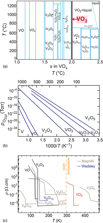
Moving from the frontier of fundamental research in VO2 electronics toward their realization in commercial products, a method to deposit high-quality and ultrathin VO2 films on wafer scale is needed. For example, memory devices based on MITs have the advantage of compact node sizes down to a few nm and VO2 films must preserve their MIT properties during the scaling process, e.g., maintaining at least four orders of magnitude change in resistivity across the MIT.[ Reference Zhou and Ramanathan 44 ] However, the MIT properties in VO2 thin films has long been recognized to be highly sensitive to deposition conditions including substrate temperature, background oxygen pressure, as well as deposition technique. This delicate nature of VO2 results from its complex phase diagram as shown in Fig. 4(a). The VO2 phase is not a line compound, and, thus, is intrinsically susceptible to point defect formation if growth conditions deviate slightly from the ideal ratio. Long-range order of these defects can occur forming distinctive phases.[ Reference Kang 45 ] In the oxygen deficient case, VO2−δ , the so-called Magnéli phases, V n O2n−1, with n = 3–7 form a homologous series with one oxygen layer missing after every nth vanadium (211) plane of the VO2 rutile structure. Similarly, the oxygen-rich VO2+δ Wadsley phases, V n O2n+1 are known with n = 2, 3, and 6.[ Reference Hirotsu and Sato 46 , Reference Katzke, Tolédano and Depmeier 47 ]

Figure 4. (a) Phase diagram of vanadium oxide, adapted permission from Ref. Reference Katzke, Tolédano and Depmeier47. Copyrighted by the American Physical Society. (b) The Ellingham diagram for vanadium oxide phases.[ Reference Barin 48 , Reference Moshfegh and Ignatiev 49 ] (c) Resistivity versus temperature for various V–O phases, with a MIT at different temperatures. While V2O3 exhibits the largest change in resistivity over eight orders of magnitude, but below room temperature, VO2 has the largest resistivity ratio above room temperature of about five orders of magnitude.[ Reference Morin 20 , Reference Feinleib and Paul 21 , Reference Chudnovskii, Terukov and Khomskii 30 , Reference Kachi, Kosuge and Okinaka 181 – Reference Okinaka, Kosuge, Kachi, Nagasawa, Bando and Takada 183 ]
The rich phase diagram, the different polymorphs and the ability to easily accommodate defects that can order and dramatically affect the MIT properties, makes the growth of a targeted vanadium oxide phase particularly challenging.[
Reference Kang
45
]
Figure 4(b) shows the Ellingham diagram calculated from the enthalpy of reaction for selected vanadium oxide phases tabulated in Refs. Reference Barin48, Reference Moshfegh and Ignatiev49. Because entropy data were not available for all of these phases, ∆S of the reactions was assumed to be zero. All lines represent thermodynamic phase equilibria of the oxidation reaction ${\rm VO}_{x(s)} + (y/2){\rm O}_{2(g)} \rightleftharpoons {\rm VO}_{x + y(s)} $
, where higher temperature and lower oxygen partial pressure stabilizes a vanadium oxide phase with a lower vanadium oxidation state. While V2O5 is the thermodynamically stable phase at ambient condition, thin-film deposition in vacuum and at elevated temperature are ideally suited to stabilize the desired VO2 phase. Notably, with sample temperatures typically ranging between 300 and 600 °C, growth by pulsed-laser depostion (PLD) in varying oxygen partial pressures has shown that a minimum background oxygen pressure of 10−2 Torr is required to avoid oxygen deficient VO2 on sapphire substrates.[
Reference Jeong, Aetukuri, Graf, Schladt, Samant and Parkin
42
] Similarly, for VO2 grown by molecular-beam epitaxy (MBE) distilled ozone background pressures of 10−6 Torr with substrate temperatures in the 200–350 °C range,[
Reference Tashman, Lee, Paik, Moyer, Misra, Mundy, Spila, Merz, Schubert, Muller, Schiffer and Schlom
50
–
Reference Paik, Moyer, Spila, Tashman, Mundy, Freeman, Shukla, Lapano, Engel-Herbert, Zander, Schubert, Muller, Datta, Schiffer and Schlom
52
] or an oxygen plasma pressure[
Reference Fan, Chen, Wu, Chen, Chu, Chen, Zou and Wu
53
] of (1–3) × 10−5 Torr at a substrate temperature of 550 °C were used.[
Reference Paik, Moyer, Spila, Tashman, Mundy, Freeman, Shukla, Lapano, Engel-Herbert, Zander, Schubert, Muller, Datta, Schiffer and Schlom
52
,
Reference Fan, Chen, Wu, Chen, Chu, Chen, Zou and Wu
53
] According to the Ellingham diagram in Fig. 4(b) in all cases V2O5 is expected to form. The discrepancy between thermodynamic equillibrium calculations and experimental conditions used for the growth of high-quality VO2 films suggests that the growth kinetics play an important role as well. A kinetic barrier to the oxidation of vanadium at the low growth temperatures used to form VO2 films has been observed in surface science experiments,[
Reference Della Negra, Sambi and Granozzi
54
] necessitating oxidation conditions that fall in the V2O5 region of the Ellingham diagram for all growth techniques. Indeed, considering the growth conditions common to VO2 films, it is plausible that some V2O5 does form during growth, but desorbs due to its high volatility[
Reference Pak
55
] leaving behind a phase-pure film of VO2 in conditions that thermodynamics indicates should be in the territory of V2O5. Growth at high substrate temperature to overcome the kinetic barrier to oxidation is not an option for two reasons: (1) the rapid interdiffusion of VO2 into the underlying substrates[
Reference Tashman, Lee, Paik, Moyer, Misra, Mundy, Spila, Merz, Schubert, Muller, Schiffer and Schlom
50
,
Reference Paik, Moyer, Spila, Tashman, Mundy, Freeman, Shukla, Lapano, Engel-Herbert, Zander, Schubert, Muller, Datta, Schiffer and Schlom
52
,
Reference Della Negra, Sambi and Granozzi
54
] and (2) if the entire film is oxidized to V2O5, it will all evaporate due to the high vapor pressure of V2O5.[
Reference Pak
55
]
${\rm VO}_{x(s)} + (y/2){\rm O}_{2(g)} \rightleftharpoons {\rm VO}_{x + y(s)} $
, where higher temperature and lower oxygen partial pressure stabilizes a vanadium oxide phase with a lower vanadium oxidation state. While V2O5 is the thermodynamically stable phase at ambient condition, thin-film deposition in vacuum and at elevated temperature are ideally suited to stabilize the desired VO2 phase. Notably, with sample temperatures typically ranging between 300 and 600 °C, growth by pulsed-laser depostion (PLD) in varying oxygen partial pressures has shown that a minimum background oxygen pressure of 10−2 Torr is required to avoid oxygen deficient VO2 on sapphire substrates.[
Reference Jeong, Aetukuri, Graf, Schladt, Samant and Parkin
42
] Similarly, for VO2 grown by molecular-beam epitaxy (MBE) distilled ozone background pressures of 10−6 Torr with substrate temperatures in the 200–350 °C range,[
Reference Tashman, Lee, Paik, Moyer, Misra, Mundy, Spila, Merz, Schubert, Muller, Schiffer and Schlom
50
–
Reference Paik, Moyer, Spila, Tashman, Mundy, Freeman, Shukla, Lapano, Engel-Herbert, Zander, Schubert, Muller, Datta, Schiffer and Schlom
52
] or an oxygen plasma pressure[
Reference Fan, Chen, Wu, Chen, Chu, Chen, Zou and Wu
53
] of (1–3) × 10−5 Torr at a substrate temperature of 550 °C were used.[
Reference Paik, Moyer, Spila, Tashman, Mundy, Freeman, Shukla, Lapano, Engel-Herbert, Zander, Schubert, Muller, Datta, Schiffer and Schlom
52
,
Reference Fan, Chen, Wu, Chen, Chu, Chen, Zou and Wu
53
] According to the Ellingham diagram in Fig. 4(b) in all cases V2O5 is expected to form. The discrepancy between thermodynamic equillibrium calculations and experimental conditions used for the growth of high-quality VO2 films suggests that the growth kinetics play an important role as well. A kinetic barrier to the oxidation of vanadium at the low growth temperatures used to form VO2 films has been observed in surface science experiments,[
Reference Della Negra, Sambi and Granozzi
54
] necessitating oxidation conditions that fall in the V2O5 region of the Ellingham diagram for all growth techniques. Indeed, considering the growth conditions common to VO2 films, it is plausible that some V2O5 does form during growth, but desorbs due to its high volatility[
Reference Pak
55
] leaving behind a phase-pure film of VO2 in conditions that thermodynamics indicates should be in the territory of V2O5. Growth at high substrate temperature to overcome the kinetic barrier to oxidation is not an option for two reasons: (1) the rapid interdiffusion of VO2 into the underlying substrates[
Reference Tashman, Lee, Paik, Moyer, Misra, Mundy, Spila, Merz, Schubert, Muller, Schiffer and Schlom
50
,
Reference Paik, Moyer, Spila, Tashman, Mundy, Freeman, Shukla, Lapano, Engel-Herbert, Zander, Schubert, Muller, Datta, Schiffer and Schlom
52
,
Reference Della Negra, Sambi and Granozzi
54
] and (2) if the entire film is oxidized to V2O5, it will all evaporate due to the high vapor pressure of V2O5.[
Reference Pak
55
]
Despite the many challenges involved in the growth of VO2 films, significant advances have been achieved in its deposition using PLD,[ Reference Jeong, Aetukuri, Graf, Schladt, Samant and Parkin 42 , Reference Koo, Yoon, Kwon, Ko, Shin, Bae, Chang and Park 56 – Reference Lee, Meyer, Park, Egami and Lee 63 ] MBE,[ Reference Paik, Moyer, Spila, Tashman, Mundy, Freeman, Shukla, Lapano, Engel-Herbert, Zander, Schubert, Muller, Datta, Schiffer and Schlom 52 , Reference Fan, Chen, Wu, Chen, Chu, Chen, Zou and Wu 53 , Reference Zhang, Zhang, Mukherjee, Zheng, Haislmaier, Alem and Engel-Herbert 64 , Reference Zhang, Eaton, Ye and Engel-Herbert 65 ] sputtering,[ Reference Cui and Ramanathan 66 – Reference Zhang, Wang, Fan, Liu, Guo, Zou, Wang, Qian, Ibrahim, Yan, Xu and Wu 73 ] electron-beam deposition,[ Reference Hood and DeNatale 74 ] ion-beam depostion,[ Reference West, Lu and Yu 75 ] metalorganic chemical vapor deposition (MOCVD),[ Reference Kim, You, Chiarello, Chang, Zhang and Lam 61 , Reference Maruyama and Ikuta 76 ] chemical solution deposition[ Reference Ji, Pan, Bi, Liang, Zhang, Zeng, Wen, Zhang, Chen, Jia and Lin 77 ] and atomic layer deposition (ALD).[ Reference Dagur, Mane and Shivashankar 78 , Reference Rampelberg, Schaekers, Martens, Xie, Deduytsche, De Schutter, Blasco, Kittl and Detavernier 79 ] Using the resistivity ratio across the MIT as a benchmark for film quality, Fig. 5 shows a comparison of VO2 films grown by different techniques from the aforementioned references. Since strain affects the resistivity ratio across the MIT as well, only fully relaxed films grown on sapphire substrates were selected here. Two general trends are observed: (1) For thick films well above 100 nm, high-quality VO2 films with MIT ratio more than four orders of magnitude are commonly achieved. (2) With decreasing film thickness, the MIT ratios deteriorate to less than two orders of magnitude. Interestingly, recent progress in PLD has demonstrated high-quality VO2 films with an MIT ratio: >5000 at film thicknesses as small as ~20 nm.[ Reference Jeong, Aetukuri, Graf, Schladt, Samant and Parkin 42 ] Also, growth of high quality VO2 thin films on large silicon wafers has been demonstrated using sputtering.[ Reference Savo, Zhou, Castaldi, Moccia, Galdi, Ramanathan and Sato 80 ] In addition, a combinatorial approach for the growth of VO2 has been developed using a thermal source for V and the metalorganic precursor vanadium-oxo-triisopropoxide to supply vanadium in a much higher valence state, which demonstrated the potential to combine high-quality VO2 at a dramatically reduced film thickness on wafer scale, while keeping a high resistivity change across the MIT intact.[ Reference Paik, Moyer, Spila, Tashman, Mundy, Freeman, Shukla, Lapano, Engel-Herbert, Zander, Schubert, Muller, Datta, Schiffer and Schlom 52 – Reference Della Negra, Sambi and Granozzi 54 , Reference Zhang, Zhang, Mukherjee, Zheng, Haislmaier, Alem and Engel-Herbert 64 ] High-quality VO2 films are a key enabler for electrical engineers to exploit the opportunities offered by electronic PCMs in general and VO2 in particular in proof-of-principle photonic and electronic devices, which are described in detail next.

Figure 5. Change in resistivity across the MIT, Δρ/ρ (indicated by various symbol) reported for completely relaxed VO2 films grown on sapphire with different thickness.[ Reference Jeong, Aetukuri, Graf, Schladt, Samant and Parkin 42 , Reference Paik, Moyer, Spila, Tashman, Mundy, Freeman, Shukla, Lapano, Engel-Herbert, Zander, Schubert, Muller, Datta, Schiffer and Schlom 52 , Reference Fan, Chen, Wu, Chen, Chu, Chen, Zou and Wu 53 , Reference Koo, Yoon, Kwon, Ko, Shin, Bae, Chang and Park 56 – Reference Maruyama and Ikuta 76 ] The dotted line indicates the thickness at which VO2 is completely relaxed. The data are grouped into the different thin-film deposition techniques, arranged from left to right with increasing scalability. Note that in general a larger film thickness results in a larger Δρ/ρ.
Augmenting field effect transistors (FETs) with VO2
In CMOS technology, the backbone of the current computing hardware, the strategy to realize low-power, high-performance computation is to reduce the total energy necessary to switch a FET from an OFF-state to an ON-state. The FET is switched by changing the gate voltage V
GS to modulate the drain-to-source current I
DS by orders of magnitude. The associated energy contains a dynamic contribution $E_{{\rm dyn}} = (\alpha /2)CV_{dd}^2 $
, with the intrinsic transistor gate capacitance C charged to turn the device into the ON state, the supply voltage V
dd
, and dimensionless activity factor α to account for the fraction of clock cycles the transistor is switched. The static contribution is given by E
stat = I
leak
V
dd
τ, with I
leak the leakage current between source and drain in the OFF-state and τ the switching period, i.e., the clock speed of the processor. Switching the transistor from OFF to ON is achieved by changing the gate voltage, and along with that the surface potential and band bending ΨS in the channel, reducing the energy barrier between source and channel thus modulating the source–drain current I
DS.
$E_{{\rm dyn}} = (\alpha /2)CV_{dd}^2 $
, with the intrinsic transistor gate capacitance C charged to turn the device into the ON state, the supply voltage V
dd
, and dimensionless activity factor α to account for the fraction of clock cycles the transistor is switched. The static contribution is given by E
stat = I
leak
V
dd
τ, with I
leak the leakage current between source and drain in the OFF-state and τ the switching period, i.e., the clock speed of the processor. Switching the transistor from OFF to ON is achieved by changing the gate voltage, and along with that the surface potential and band bending ΨS in the channel, reducing the energy barrier between source and channel thus modulating the source–drain current I
DS.
Even in the OFF-state thermally excited carriers can overcome this barrier, captured by the Boltzmann factor exp−Δ/k B T with k B the Boltzmann constant, T the absolute temperature, and Δ the barrier height relative to the Fermi level. The resulting energy dissipation is approximately E stat = E leak ∝ V dd e −V dd / S with S is the subthreshold slope.[ Reference Ionescu and Riel 81 ] To ideally balance both contributions to the switching energy per cycle an optimal supply voltage V dd , typically close to the transistor threshold voltage is chosen; see Fig. 6. While the transistor would suffer energy losses due to the high leakage energy E stat for too small operation voltages V dd , too high V dd values would unnecessarily increase the dynamic contribution E dyn.

Figure 6. (a) Energy per cycle and (b) source–drain current I DS versus gate voltage V GS in units of the supply voltage V dd for transistors with two different subthreshold slopes S of 60 meV/dec. (limit of the Boltzmann switch), and strongly correlated Landau switch with S = 30 meV/dec.
Aside from the supply voltage, another key parameter of transistor performance is the subthreshold slope S. It describes the required change in gate voltage to achieve an order of magnitude change in the source–drain current[ Reference Jain and Alam 82 ]
 $$S = \displaystyle{{\partial V_{{\rm GS}}} \over {\partial ({\rm log}I_{{\rm DS}} )}} = \displaystyle{{\partial V_{{\rm GS}}} \over {\partial \psi _{\rm S}}} \cdot \displaystyle{{\partial \psi _{\rm S}} \over {\partial (logI_{{\rm DS}} )}} = \eta \cdot \upsilon, $$
which can be separated into the two contributions η and ν: The body factor η describes the coupling of the gate voltage V
GS to the band bending ΨS in the channel η = ∂V
GS/∂ψS = 1 + (C
s
/C
ox
), with C
s
and C
ox
the semiconductor and gate oxide capacitances, respectively. The transport factor ν relates band bending ΨS to the source–drain current I
DS. In conventional semiconductor materials, the transport factor ν is intrinsically limited by the carrier statistics through the Boltzmann factor 10−Δ/k
B
T
. Modulating the source–drain current through changes in the gate voltage entails the subthreshold slope as conversion factor $I_{{\rm DS}}\sim 10^{ - \Delta /k_{\rm B}T}\sim 10^{ - {\rm \psi }_{\rm S}/S}$
with subthreshold slope S ≥ (q/k
B
T), where q is the elemental charge. In other words, a minimum requirement of ~60 mV change in Ψ
S
is needed to modulate the source–drain current at room temperature by one order of magnitude: the famous 60 mV/decade limit of conventional FETs.[
Reference Sze and Ng
83
] This further implies that for a suitably large distinction between the OFF-state and the ON-state current, the supply voltage must be several times this limit. Consequently, the Boltzmann factor constrains supply voltage scaling, and, therefore, the switching energy of a conventional FET.
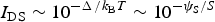
$I_{{\rm DS}}\sim 10^{ - \Delta /k_{\rm B}T}\sim 10^{ - {\rm \psi }_{\rm S}/S}$
with subthreshold slope S ≥ (q/k
B
T), where q is the elemental charge. In other words, a minimum requirement of ~60 mV change in Ψ
S
is needed to modulate the source–drain current at room temperature by one order of magnitude: the famous 60 mV/decade limit of conventional FETs.[
Reference Sze and Ng
83
] This further implies that for a suitably large distinction between the OFF-state and the ON-state current, the supply voltage must be several times this limit. Consequently, the Boltzmann factor constrains supply voltage scaling, and, therefore, the switching energy of a conventional FET.
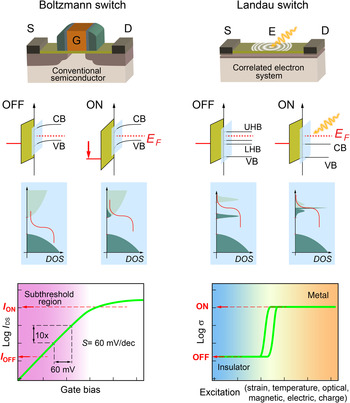
Reducing the operating voltage and energy while maintaining performance, i.e., the switching delay and a specific ON/OFF ratio, transistors with a subthreshold slope <60 mV/decade, referred to as steep-slope transistors,[ Reference Ionescu and Riel 81 , Reference Zhirnov and Cavin 84 , Reference Lu and Seabaugh 85 ] is therefore demanded. To achieve a subthreshold slope S < 60 mV/decade with η < 1 the integration of a ferroelectric layer into the gate stack to augment the linear gate dielectric has been proposed and is currently being explored.[ Reference Salahuddin and Datta 86 – Reference Catalan, Jiménez and Gruverman 90 ] The ferroelectric capacitor in series with the dielectric gate capacitor is designed to stabilize an otherwise energetically disfavored reversal pathway that entails an overall negative gate oxide capacitance effect, reversing the sign of C ox and resulting in a body factor, η, smaller than unity.
Another approach to achieve subthreshold slopes smaller than 60 mV/decade is to harness transport phenomena to directly beat the Boltzmann limit, hence improving the transport factor ν. Within the realm of conventional semiconductors, interband tunneling across semiconductor heterojunction [tunnel field effect transistor (TFETs)][ Reference Pandey, Madan, Liu, Chobpattana, Barth, Rajamohanan, Hollander, Clark, Wang, Kim, Gundlach, Cheung, Suehle, Engel-Herbert, Stemmer and Datta 91 ] and carrier multiplication via impact ionization[ Reference Gopalakrishnan, Griffin and Plummer 92 , Reference Gopalakrishnan, Woo, Jungemann, Griffin and Plummer 93 ] in metal oxide semiconductor structures (I-MOS) offer opportunities toward steep-slope switching. The I-MOS concept relies on impact ionization in an ungated intrinsic region between the source region and the channel to induce carrier amplification, which subsequently enables a larger change in current in comparison with conventional CMOS transistors for a given change in gate voltage. Scaling the supply voltage to reduce the energy per cycle, however, is not possible for I-MOS, which along with its disadvantages, namely dead region in the output region precluding inverter operation, reliability issues due to hot carrier formation potentially damaging the dielectric, renders this design unsuitable for high-performance low-power transistors. TFETs utilize a gate tunable tunnel junction in which the conduction and valence band alignment across the heterojunction is modulated, which results in steep turn-ON characteristics for carriers entering the channel from the source.[ Reference Ionescu and Riel 81 , Reference Theis, Solomon, Dennard, Gaensslen, Rideout, Bassous, LeBlanc, Haensch, Banerjee, Richardson, Coleman, Chatterjee, Appenzeller, Lin, Knoch, Avouris, Salahuddin, Datta, Li, Kopp, Mannhart, Mannhart and Schlom 94 ] Relying on tunneling phenomenon as injection mechanism limits the source–drain current I DS in the ON state and thus its suitability for high-performance computing where high ON currents are required.
Nevertheless, the modulation of the band alignments at the heterojunction is a powerful concept, which suggests an alternative pathway to overcome the Boltzmann limit by employing materials exhibiting electronic phase transitions, as schematically shown in Fig. 7. In contrast to conventional semiconductors, where the electronic bands are only shifted with respect to the Fermi level by an electric field, carriers in correlated electron system can change their character from localized to itinerant and the entire band structure is altered in the vicinity of the Fermi level. Rather than a Boltzmann switch in case of conventional FETs, the concept is best coined as a “Landau switch” in the sense that switching characteristics is not governed by carrier statistics anymore, but rather by the free energy of the competing phases with different electronic ground states. Materials exhibiting strong correlations are therefore uniquely suited to overcome the intrinsic limit of conventional Boltzmann switches by harnessing electronic phase transition. The external perturbation triggering the electronic phase transformation between different ground states does not necessarily have to be an electric field, but could be strain, magnetic field, optical excitation, or other thermodynamic variables, such as temperature or pressure,[ Reference Inoue and Rozenberg 95 , Reference Hwang, Iwasa, Kawasaki, Keimer, Nagaosa and Tokura 96 ] all of those offering novel opportunities toward steep-slope-transistor functionalities.

Figure 7. A comparison of the properties of the currently employed Boltzmann switch as FETs (left), which switch state by changing the Fermi level E F relative to the band structure unaltered by the electric field. The concept of a Landau switch is shown on the right, which is envisioned to operate by changing the DOS at the Fermi level by triggering an electronic phase transition through various external stimulations. Such functionality could overcome the 60 mV/dec. limit intrinsic to conventional FETs semiconductors, enabling low-power, high-performance computing with ultrascaled supply voltages.
The Mott-FET[ Reference Newns, Misewich, Tsuei, Gupta, Scott and Schrott 97 – Reference Kim, Chae, Youn, Maeng, Kim, Kang and Lim 100 ] is a concept in which the semiconducting channel of a conventional transistor is replaced by a phase transition material, for example VO2. The operating principles are as follows: the transistor is initially OFF when the phase transition material is in the high-resistance insulating state. When a sufficient gate field is applied accumulation of free carriers at the dielectric/Mott-material interface screens the Coulomb repulsion among the localized carriers in the insulating state of VO2. Consequently, the electric field triggers an abrupt carrier delocalization inducing the low resistance metallic state. The abrupt liberation of all carriers previously localized to atomic sites enables the transistor to exhibit a sharp turn-on characteristics with S < 60 mV/decade. Attempts to reverse the phase transition by applying an electric field to recapture the insulating ground state and to turn the transistor OFF only had limited success. The external field cannot effectively penetrate into the channel material with metallic-like carrier concentration due to the short Angstrom-scale screening length.[ Reference Martens, Jeong, Aetukuri, Rettner, Shukla, Freeman, Esfahani, Peeters, Topuria, Rice, Volodin, Douhard, Vandervorst, Samant, Datta and Parkin 101 ] The switching has to be bidirectional. The combination of ultrathin films und large field strengths using an ionic liquid gate exhibited very slow switching characteristics,[ Reference Nakano, Shibuya, Okuyama, Hatano, Ono, Kawasaki, Iwasa and Tokura 41 , Reference Zhou and Ramanathan 102 ] hinting that unintentional ionic exchange reactions affecting the channel stoichiometry might be at play as well.[ Reference Jeong, Aetukuri, Graf, Schladt, Samant and Parkin 42 ] The straight forward strategy of a Mott-FET to simply replace the semiconductor material in the channel with a strongly correlated material exhibiting an MIT is thwarted by these roadblocks.
To nevertheless harness the abrupt changes of electronic phase transition materials (EPTMs) while circumventing the field effect requirement, the concept of the Hyper-FET has been proposed and demonstrated using VO2.[ Reference Shukla, Thathachary, Agrawal, Paik, Aziz, Schlom, Gupta, Engel-Herbert and Datta 103 ] Rather than using the MIT material in the channel, the conventional FET is augmented by integrating VO2 directly into the source of the conventional MOSFET, as schematically shown in Fig. 8(a). The device design of the Hyper-FET concept ideally integrates abrupt switching phenomenon of VO2 with the superior transport characteristics of a semiconductor channel material, while circumventing the problem of bidirectional electric field switching of VO2. The operation of the Hyper-FET can be described as follows. Initially, at gate voltage V GS = 0 V, the transistor is in the OFF state with a small channel current I DS that is further reduced by the high resistance state of VO2. Increasing gate voltage as V GS increases I DS until a critical value is reached, which switches VO2 into the metallic state, thereby lowering the series resistance and abruptly increasing I DS; see Fig. 8(b). Similarly, as V GS is reduced, the channel current decreases until a lower critical current is reached at which VO2 transitions back into the high resistance state. The Hyper-FET exhibits a feedback enhanced gate field controlled abrupt switching characteristics due to the phase transition in VO2 with the switching slope of 12 mV/decade at room temperature.[ Reference Shukla, Thathachary, Agrawal, Paik, Aziz, Schlom, Gupta, Engel-Herbert and Datta 103 ] The steep switching slope enables this hybrid phase-transition-FET to achieve higher ON current at matched OFF currents in comparison with conventional MOSFETs. The Hyper-FET primarily enables steep slope operation by achieving a transport factor ν = [∂ψS/∂(logI DS)] less than 60 mV/decade at room temperature due to orders of magnitude abrupt change in resistance in the source, and, thus, providing a much larger current change ∂(logI DS) for an infinitesimally small increment in the channel potential ∂ψS.

Figure 8. (a) Schematic representation of the Hyper-FET wherein an electronic PCM exhibiting an electronically induced abrupt change in resistivity (such as VO2) is integrated in series with the source of a conventional MOSFET. (b) Transfer characteristics (I DS–V GS) of the VO2-based Hyper-FET at room temperature. (c) Switching slope S of the Hyper-FET as a function of drain-to-source current I DS demonstrating a sub-k B T/q switching-slope (i.e., <60 mV/dec) at room temperature [panels (a) and (b) are adapted from Ref. Reference Shukla, Thathachary, Agrawal, Paik, Aziz, Schlom, Gupta, Engel-Herbert and Datta103].
The EPTM integrated into the source of the FET is not restricted to VO2, the device design is scalable and has also been demonstrated using In0.7Ga0.3As quantum-well multi-channel FinFETs for n-MOS and complimentary p-MOS using a Ge quantum-well multi-channel FinFETs.[ Reference Shukla, Thathachary, Agrawal, Paik, Aziz, Schlom, Gupta, Engel-Herbert and Datta 103 ]
While proof-of-principle has been demonstrated, technological challenges to implement this device concept into mainstream technology remains to be addressed. First, it needs to be demonstrated that aggressive scaling of the Hyper-FET design to below 10 nm can be achieved with maintaining a sizeable, (i.e., few orders of magnitude) resistivity change across the MIT of VO2; this then favorably reflects into transfer characteristics with much larger source–drain current for a fixed, small gate voltage modulation. Further, given that the MIT in VO2 is affected by temperature, a potential sensitivity of transfer characteristics to the chip temperature when implemented in portable electronics, and more under heavy computation loads when large amounts of heat are being dissipated, are additional practical concerns to be addressed in the future. While VO2 might not be an ideal materials solution for the application, the task for material scientists will be to find a better suited electronic PCM that allows for scaling and for a more seamless integration into the existing fabrication process. The concept of the Hyper-FET uniquely combines the abrupt collective carrier response from phase transition materials arising from strong electron correlation present in small band width material with the superior carrier transport characteristics in semiconductor materials stemming from the small carrier effective mass enabled by a large band width, while avoiding the need to directly induce the phase transition by an electric field. It therefore represents an ideal symbiosis of the two entirely different material classes of semiconductors and electronic PCMs.
Non-Boolean computing using charge coupled VO2 oscillators
While in the Hyper-FET concept the MIT material has merely the role to augment, it dramatically improved the conventional FET characteristics dominated by the semiconductor channel by utilizing the abrupt resistivity change of VO2. A completely different aspect of computation, namely associative computing, has been explored and can be potentially harnessed if the attention is focused back on the two-terminal VO2 device as the active element and simplifying the function of the FET in series to that of a tunable resistor R s, as shown in Fig. 9(a). The abrupt and hysteretic evolution of current passing through VO2 as a function of applied voltage encompasses the fundamental instability of the first order phase transition, separating the insulating from the metallic state. In the case of a negligible series resistance R S the insulator-to-metal transition (IMT), i.e., the transition from the insulating to the metal state of VO2 is triggered at a critical field strength of E 2 = V 2/L, determined from the voltage drop V 2 across VO2 and the electrode distance L; see Fig. 9(b). The applied voltage has to then be reduced to E 1 = V 1/L to reverse the transition, i.e., going from the metallic back to the insulating state (MIT) to obtain the high resistance state again. Small series resistances will merely affect this hysteretic switching behavior. However, the abrupt reduction of the VO2 resistance at the critical field E 2 will redistribute the voltage drops across the series resistor R S and the VO2 device. Triggering the metallic state in VO2 results in an instantaneous current increase and reduction of the voltage across the VO2 device, thus acting as a negative differential resistance. For a series resistance above the critical value R C the change in voltage drop across the VO2 device is so high that the remaining field strength is less than the critical field E 1 required to stabilize the metallic state. Under these conditions and even though the metallic state was nucleated at the critical field value E 2, the high resistance state in VO2 cannot be completely annihilated. Rather, the low electric field now favors the insulating state of VO2, reversing the transition. This in turn increases the device resistance, and, with it the voltage drop across VO2 device, again favoring the metallic state. The sufficiently large series resistance stabilizes VO2 into a non-hysteretic phase coexistence regime, defined within the bounds of the critical field values E 2 and E 1, which are strongly temperature dependent; see Fig. 9(c). The waveform of the oscillation induced by a DC signal is shown in Fig. 9(d), which has been measured by probing the voltage drop V R across the series resistor [Fig. 9(a)]. An increase in V R is found upon decreasing the VO2 resistance (IMT), while a reduction of V R is associated with a resistance increase of VO2 (MIT). The associated time constants for the IMT and the MIT of τ 1 (0.35 µs) and τ 2 (0.65 µs), respectively, were dominated by parasitic resistances and capacitances present in the simple experimental setup, and thus orders of magnitude larger than the intrinsic time constants of the VO2 phase transition.[ Reference Wen, Guo, Barnes, Lee, Walko, Schaller, Moyer, Misra, Li, Dufresne, Schlom, Gopalan and Freeland 104 ] Reducing the series resistance R S increased the frequency of the VO2 oscillation, Fig. 9(e). A continuous change in the R S can be achieved by replacing R S with a transistor and adjusting its channel resistance using the gate voltage V GS, Fig. 9(f).

Figure 9. (a) Schematic representation of the VO2-based relaxation oscillator: a two-terminal VO2 device in series with a resistor R S. (b) Current versus voltage characteristics of the VO2 device: no R S (black), R S < R C (red load line 2), and with R S > R C (blue load line 1). While hysteretic transition and abrupt change in current is found for R S < R C, a non-hysteretic transition with oscillations is observed for R S > R C. (c) Temperature dependence of the critical electric-fields E 2 and E 1 for VO2 devices grown on (001) TiO2. An intermediate region of phase coexistence of both, the insulating and metallic phases was accessible, enabling the oscillatory behavior of VO2. (d) Typical time-domain wave form of the VO2-based relaxation oscillator. Inset shows the one oscillation period with the two time constants (τ 1 = 0.35 and τ 2 = 0.651 µs) associated with the IMT and the MIT. (e) Effect of input voltage V in and series resistor R S on the operating frequency of the oscillator. (f) Frequency versus gate voltage V GS characteristics of a voltage-controlled VO2 oscillator constructed by replacing R S with a MOSFET; allowing to tune the series resistance using V GS [panels (b), (c), (e), and (f) are adapted from Ref. Reference Shukla, Parihar, Freeman, Paik, Stone, Narayanan, Wen, Cai, Gopalan, Engel-Herbert, Schlom, Raychowdhury and Datta184, and (d) is adapted from Ref. Reference Shukla, Parihar, Cotter, Barth, Li, Chandramoorthy, Paik, Schlom, Narayanan, Raychowdhury and Datta110].
Coupling these highly scalable, inductor-free voltage controlled charge oscillator devices and investigating the synchronization dynamics of those coupled devices could open up opportunities to realize a simple hardware platform for a specific class of computing problems, referred to as associative computing.[ Reference Türel, Lee, Ma and Likharev 105 ] Compared with sequential algorithms developed for conventional CMOS hardware the synchronization dynamics of coupled oscillators, an inherently parallel process, could be potentially used to solve computationally hard problems more efficiently. Such tasks range from combinatorial optimization problems like graph coloring[ Reference Wu 106 ] or the traveling salesman problem,[ Reference Lawler, Lenstra, Rinnooy Kan and Shmoys 107 ] and include associative computating problems related to image and pattern recognition,[ Reference Hölzel and Krischer 108 – Reference Shukla, Parihar, Cotter, Barth, Li, Chandramoorthy, Paik, Schlom, Narayanan, Raychowdhury and Datta 110 ] as well as scene segmentation and saliency detection problems using the concept of oscillatory locally excitatory globally inhibitory networks[ Reference Wang and Terman 111 ] required in computer vision systems.
To investigate the coupling behavior of VO2 oscillators, two devices were stabilized at different frequencies of 48.43 and 37.27 kHz by choosing different values of R S (38 and 47 kΩ). Figure 10(a) schematically shows how both elements were linked using a capacitor (C C = 680 pF) as the coupling element. The different operating frequencies of each oscillator prior to coupling shown in Fig. 10(b) indicated that the oscillators were completely independent. After pairing them with the coupling capacitor, the oscillators synchronized to a common resonant frequency. A narrowing of the spectral line width further corroborated the locking of the two oscillators and the presence of a mutual feedback stabilizing the synchronized oscillator pair against noise. Figure 10(c) shows the time evolution of the coupled resistance states of both oscillators, 1 and 2. Tracing the trajectory in the phase diagram by using the voltage drops V R,1 and V R,2 across both series resistances R S,1 and R S,2 allowed one to determine the metallic-to-insulating phase ratio in the individual devices. As device-1 transitioned from the insulating toward the metallic phase, device-2 changed from the metallic to the insulating state [Section “Strong electron correlations in V-based oxides” of the phase space trajectory in Fig. 10(c)]. Conversely, when device-1 was in a more metallic and device-2 was in a more insulating state, charge was exchanged through the coupling capacitance and moved from device-1 to device-2, represented by the Section “Ternary oxide vanadates” of the trajectory in Fig. 10(c).

Figure 10. (a) Schematic of the capacitively coupled VO2 oscillators. (b) Spectral characteristics of the oscillators before and after capacitive coupling. The individual oscillators synchronize to a common resonant frequency when coupled. (c) Simulated phase space trajectory of the coupled oscillators. The evolution of phase composition in the coupled VO2 devices is determined from V R,1 and V R,2. Coupled oscillators predominantly show out of phase locking with one oscillator in the metallic state, while the other is in the insulating state. (d) Schematic representation of a pair of voltage tunable coupled VO2 oscillators wherein R S is replaced by a transistor with gate voltage tunable channel resistance. (e) Phase space trajectory of the coupled VO2 oscillators as function of gate voltage difference V GS,2–V GS,1. As the degree of similarity between the inputs decreases V GS2–V GS1 becomes larger (inputs are similar when V GS,2–V GS,1 = 0) and the oscillators exhibit increased in-phase locking behavior (shaded area in the V R,1–V R,2 phase space). (f) Simulated time average XOR output of the coupled oscillators, and (g) L 1/2 distance norm as a function of V GS,1 and V GS,2. The qualitative match between the XOR output and the L 1/2 distance norm indicates that the XOR output of the coupled oscillators resembles the nonlinear distance norm of the Euclidean space [panels (b) and (c) are adapted from Ref. Reference Shukla, Parihar, Freeman, Paik, Stone, Narayanan, Wen, Cai, Gopalan, Engel-Herbert, Schlom, Raychowdhury and Datta184, and (e)–(g) are adapted from Reference Shukla, Parihar, Cotter, Barth, Li, Chandramoorthy, Paik, Schlom, Narayanan, Raychowdhury and Datta110].
The precise shape of phase space trajectories of the coupled oscillator pair has been found strongly dependent on the difference of the series resistances R S,1 and R S,2. Therefore, as shown in Fig. 10(d), replacing the resistors by conventional MOSFETs and using the gate voltages V GS,1 and V GS,2 as input parameter, their degree of match is decoded into a specific shape of the trajectory in the V R,1–V R,2 phase space. While for large differences in the input voltages V GS,1 and V GS,2 no stable trajectory was formed—the oscillator pair did not sychronize—smaller differences ΔV = V GS,2–V GS,1 dramatically altered the trajectory, as schematically depicted in Fig. 10(e). To analyze these changes and form a simple output value from the coupled oscillator pair an average exclusive-OR (XOR) measure applied to V R,1 and V R,2 was used; a time-equivalent metric to quantify how long the coupled oscillators remained in the gray-shaded area in phase space during an oscillation period, as indicated in Fig. 10(e). While the XOR values were small for ΔV ≈ 0, the nonlinear increase with ΔV shown in Fig. 10(f) closely resembled the Euclidean norm L 1/2 = (X 1 2 + X 2 2)1/2 shown in Fig. 10(g).
This sensitivity of the coupled oscillators’ phase space orbit to the difference in the input parameters forms the basic computational hardware building block of the coupled oscillators. A non-linear distance norm[ Reference Parihar, Shukla, Datta and Raychowdhury 112 ] that can be used to determine how closely the two analog voltage input values resemble each other is realized by the simple hardware building block of capacitively coupled two-terminal electronic PCM, allowing for fast and energy-efficient computation of tailored non-linear degree-of-match-type analysis.[ Reference Shukla, Parihar, Cotter, Barth, Li, Chandramoorthy, Paik, Schlom, Narayanan, Raychowdhury and Datta 110 , Reference Parihar, Shukla, Datta and Raychowdhury 112 ] This task will play a critical role in the paradigm shift from precise computing on small data sets to approximate computing on large data sets, which has already occurred in future application areas, such as machine learning, augmented reality, and data base search.[ Reference Watts and Strogatz 113 ] A dramatically increasing demand to solve this task elegantly in a fast, computationally inexpensive, and thus, energetically efficient way, is projected for data analysis generated from massive sensor arrays in the dawning IOT (internet-of-things) era. Two-terminal devices made from electronic PCM exhibiting current-controlled resistive switching have been identified as key in neuristors[ Reference Pickett, Medeiros-Ribeiro and Williams 114 ] to mimic biological functionality of neural networks using solid-state electronic circuitry, a further evidence of the critical role of these types of materials to meet future computation demands.
VO2 as RF switch
Currently state-of-the-art switches can be categorized into MEMS and solid-state devices, both of which enable switching between a high-impedance (OFF) state and a low-impedance (ON) state for RF frequency signals. One of the key performance parameter of an RF switch is the cut-off frequency, f CO, at which the ratio of impedance of the ON state and OFF state is unity, thus defining the maximum operating frequency
 $$f_{{\rm CO}} = (2\pi R_{{\rm ON}} C_{{\rm OFF}} )^{ - 1}, $$
with R ON is the ON state resistance, and C OFF is the OFF state capacitance.While solid-state semiconductor-based RF switches are limited to f CO at least 2–3 orders lower than MEMS switches due to their comparably high R ON and high C OFF, their low drive voltage, high switching speed, and excellent reliability due to no moving mechanical parts render them a highly competitive solution. Near zero power consumption, high electrical isolation in the OFF state, very low insertion losses, high cut-off frequencies, and highly linear performance make MEMS switches attractive, compensating for their low switching speeds, high voltage, or current drive needed to actuate the switch despite their higher fabrication costs and lower reliability. The ideal RF switch would be a combination of both approaches, a simple solid-state design exhibiting a fast-switching characteristics along with a MEMS-like high frequency of operation and low insertion loss.
One approach to realize such an RF switch is to harness the change in resistivity across the MIT in TMOs such as VO2. Demonstrations and benchmarking of VO2-based RF switches have been done using films grown by pulse laser deposited (PLD)[ Reference Dumas-Bouchiat, Champeaux, Catherinot, Crunteanu and Blondy 115 ] and sputtering.[ Reference Ha, Zhou, Fisher, Ramanathan and Treadway 116 ] While these deposition techniques produce films with varying degree of crystallinity and strain, a relatively low R OFF/R ON ratio and increase in device capacitance due to grain boundaries causing undesirable parasitic contributions and reducing C OFF are expected to detrimentally affect device performance. For the best performance single-crystalline VO2 films with a large change in the resistivity across the MIT grown on a low loss substrate using a scalable deposition technique is desired. Figure 11(a) shows a false-colored secondary electron micrograph of a solid-state RF switch. A ground-signal-ground (GSG) pad structure consisting of 24 parallel two-terminal VO2 devices with 1 µm width and 100 nm length was fabricated from a 30-nm-thick single-crystalline VO2 film with resistivity ratios larger than 104 grown on sapphire using a combinatorial growth approach.[ Reference Zhang, Zhang, Mukherjee, Zheng, Haislmaier, Alem and Engel-Herbert 64 ] Similar to the Hyper-FET concept, the transition to the low impedance metallic state was triggered by applying a DC current. A critical current of 5 mA was needed to destabilize the high impedance state. An attenuation change due to the MIT in VO2 for a 1 GHz signal from 35 dB in the OFF state (I DC = 0 mA) to 0.55 dB in the ON state (I DC = 25 mA) was measured. Figure 11(b) shows the switching response of the device for a 50 MHz RF signal and a 250 ns pulse of 2 V amplitude to activate the switch. A fast turn-on characteristic of 25 ns was found along with an excellent endurance without observing device breakdowns after cycling between ON and OFF states for more than 108 times, shown in Fig. 11(c).

Figure 11. (a) False-colored scanning electron micrograph (SEM) of a VO2-based solid-state RF switch, a two-terminal GSG structure made up of 24 parallel channels, each with a width of 1 µm and length of 100 nm. (b) Turn ON characteristics of the VO2-based RF switch with a DC activating pulse (black) and 50 MHz RF signal (green). The output pulse (red) shows that the switch can be turned ON in <25 ns. (c) Endurance test of the solid-state VO2 RF switch. Stable R ON/R OFF ratio (normalized to the first cycle) is observed for close to one billion cycles. (d) Performance benchmarking of various RF switch technologies, comparing the typical OFF-state capacitance (C OFF) at a specified ON-state resistance (R ON);[ Reference Howell, Stewart, Freitag, Parke, Nechay, Harlan, King, Gupta, Hartman, Borodulin, Snook, Wathuthanthri, Ralston, ReNaldo and Henry 119 – Reference Mennai, Bessaudou, Cosset, Guines, Blondy and Crunteanu 126 ] the color scale represents the cut-off frequency f co. PCMs and EPTMs, such as VO2, ideally combine the superior performance of MEMS with the reliable and fast switching characteristics of solid-state switches [panels (a)–(d) are adapted from Ref. Reference Madan, Zhang, Jerry, Mukherjee, Alem, Engel-Herbert and Datta118].
These testaments of fast response and reliability of the VO2-based solid-state RF switch are ideally complemented by a high cut-off frequency of 26.5 THz, enabled by the low insertion loss of metallic VO2 in the ON state and a large OFF state capacitance due to excellent microstructural properties of the grown VO2 films. Compared with a state-of-the-art GaN based solid-state RF switch using a superlattice structure with a castellated three-dimensional (3D) gate[ Reference Nechay, Howell, Stewart, Parke, Freitag, Cramer, King, Gupta, Hartman, Borodulin, Snook, Wathuthanthri, Renaldo and Henry 117 ] a 10 dB improvement in the switching ratios for a 20 GHz signal highlights the potential of VO2-based RF switches for high-frequency signal operation, outperforming conventional solid-state FET designs, and III–V-based high-electron-mobility transistors (HEMTs).[ Reference Madan, Zhang, Jerry, Mukherjee, Alem, Engel-Herbert and Datta 118 ] Figure 11(d) compiles cut-off frequencies of several MEMs and solid-state RF switching technologies with PCM and VO2.[ Reference Howell, Stewart, Freitag, Parke, Nechay, Harlan, King, Gupta, Hartman, Borodulin, Snook, Wathuthanthri, Ralston, ReNaldo and Henry 119 – Reference Mennai, Bessaudou, Cosset, Guines, Blondy and Crunteanu 126 ] While VO2 devices were also operated using local heating, which revealed a higher cut-off frequency of f CO = 44 THz, the turn-on characteristics is expected to be not as competitive due to the necessity to integrate an in-line resistive heater. While the technology for integrated local heater elements have been developed and demonstrated for PCMs such as GeTe,[ Reference El-Hinnawy, Borodulin, Jones, Wagner, King, John Mason, Bain, Paramesh, Howell, Lee and Young 122 ] which also suffer from the requirement of a continuous DC power during the ON-state, longer switching times and isolation challenges due to RF leakage through the resistive heater in the OFF state are avertible complications of this design. Thus, EPTMs in general and VO2 on sapphire in particular provide a viable path toward realization of high-performance RF switches, ideally combining the MEMS-like high frequency of operation with reliability and fast switching characteristics of a solid-state design, harnessing the favorable properties of a MIT in this application.
Ternary oxide vanadates
The previous section (MIT in binary vanadium compounds: VO2 and V2O3) was focused on the binary oxides of vanadium V x O y in general and VO2 in particular. Their crystal structure is built from a particular geometrical arrangement of oxygen octahedra coordinating vanadium exhibiting different connectivity. If, however, a third element, such as Sr, Ca, or a rare-earth cation, is added in a 1:1 stoichiometric ratio to vanadium, the oxygen octahedron connectivity changes from a combination of corner-, edge-, and side-sharing arrangement to the solely corner-sharing ABO3 perovskite structure to make room to accommodate the large A-site cation. The perovskite unit cell is shown in Fig. 12, containing a single oxygen ochaedron with oxygen at the face center, the A-site at the corners, the B-site at the body-center. The perovskite structure can host many combinations of different elements occupying the A- and B-sites thereby encompassing a large diversity of physical properties.[ Reference Goodenough 11 , Reference Hellwege and Hellwege 127 ] Here, we focus on vanadate materials with perovskite structure, i.e., systems in which vanadium occupies the B-site. Despite the simple connectivity in this crystal structure, many structural variants from this high-symmetry cubic structure are known,[ Reference Glazer 128 – Reference O'Keeffe and Hyde 131 ] which can be thought of as displacements of the cations and tilts, rotation, stretching or compression of the oxygen octahedra without losing the corner connectivity. The small deviations in the V–O–V bond length and bond angle have dramatic effects on the charge, spin, and orbital order and thus the electronic ground state.[ Reference Rondinelli, May and Freeland 132 ]

Figure 12. Prototypical crystal structure of the ABO3 perovskite. (a) Cubic unit cell of an undistorted perovskite unit cell, consisting of a single oxygen octahedral unit that coordinates the central V-atom. (b–d) Projections along the pseudocubic axes of an orthorhombically distorted perovskite (space group Pbnm). The symmetry lowering is reflected by a unit cell doubling.
To describe and understand these structural distortions intuitively Glazer's notation is commonly employed.[
Reference Glazer
128
,
Reference Glazer
129
] A pseudocubic unit cell is used accommodating rotations of the oxygen octahedra about the three cubic axes with adjacent octahedron either in-phase or out-of-phase. The notation uses a triplet with superscripts to specify lattice parameter and rotation pattern of the oxygen octahedra, respectively. For example, SrVO3 is cubic (space group: Pm $\bar 3$
m) with a = b = c = 3.842 Å, i.e., no tilt or rotation, which is described in Glazer's notation as a
0
a
0
a
0; in contrast, CaVO3 and RVO3 (R is a rare-earth element) are both orthorhombically distorted (space group: Pbnm), exhibiting the octahedral distortion pattern a
−
a
−
c
+. Rotations about the x- and y-axes are the same and alternate between positive and negative rotations for adjacent octahedra along these axes, indicated by a−
(see lower panels in Fig. 12). In contrast, the rotation about the z-axis is in-phase (see upper right panel, Fig. 12). These subtle structural distortions are important in tuning electron correlation effects in perovskite vanadates.
$\bar 3$
m) with a = b = c = 3.842 Å, i.e., no tilt or rotation, which is described in Glazer's notation as a
0
a
0
a
0; in contrast, CaVO3 and RVO3 (R is a rare-earth element) are both orthorhombically distorted (space group: Pbnm), exhibiting the octahedral distortion pattern a
−
a
−
c
+. Rotations about the x- and y-axes are the same and alternate between positive and negative rotations for adjacent octahedra along these axes, indicated by a−
(see lower panels in Fig. 12). In contrast, the rotation about the z-axis is in-phase (see upper right panel, Fig. 12). These subtle structural distortions are important in tuning electron correlation effects in perovskite vanadates.
This section first discusses electron correlation effects in the d 1 correlated metals SrVO3 and CaVO3, followed by the challenges and recent advances in the growth of thin films of the AVO3 perovskite vanadates. In this context, emphasis is placed on how electron correlations could be further enhanced to drive these metals exhibiting strong electron correlations across the MIT to realize a vanadate based d 1 Mott-insulating phase. It is then reviewed how electron correlation can be harnessed even far away from any electronic phase transition if the metallic ground state is present. Both correlated metals SrVO3 and CaVO3 are representative of a new class of transparent conducting materials, which are critical components in all current display and photovoltaic technologies. This new class of transparent conductor (TC) is based on a novel design paradigm beyond the conventionally employed scheme to degenerately dope wide band gap semiconductors. Here, rather than increasing carrier concentration, mass enhancement of delocalized carriers in a high-density electron liquid is used to reduce the plasma frequency to below the visible spectrum.[ Reference Zhang, Zhou, Guo, Zhao, Barnes, Zhang, Eaton, Zheng, Brahlek, Haneef, Podraza, Chan, Gopalan, Rabe and Engel-Herbert 133 ] Changing the electronic configuration of perovskite vanadates from d 1 to d 2 by substituting divalent Sr and Ca by trivalent rare-earth ions, the correlation strength is substantially increased with respect to the conduction band width W and a Mott-insulating phase emerges along with interesting coupling of spin and orbital DOF that is sensitive to structural distortion. LaVO3, a representative of rare-earth vanadates exhibiting a ~1.1 eV Mott gap, will be discussed as a new absorber material for an all oxide solar cell.
Correlation effects in d 1-filled SrVO3 and CaVO3
Both SrVO3 and CaVO3 are correlated metals with a nominal 3d 1 configuration. The strong correlation properties are seen by a reduced band width compared with density functional theory calculations, as measured by angle-resolved photoemission spectroscopy.[ Reference Yoshida, Tanaka, Yagi, Ino, Eisaki, Fujimori and Shen 134 , Reference Yoshida, Kobayashi, Yoshimatsu, Kumigashira and Fujimori 135 ] As schematically shown in Fig. 2, the spectral weight transfer feature from the coherent quasi-particle peak to incoherent side bands has been experimentally observed in photoemission experiments,[ Reference Fujimori, Hase, Namatame, Fujishima, Tokura, Takegahara and de Groot 136 – Reference Mossanek, Abbate, Yoshida, Fujimori, Yoshida, Shirakawa, Eisaki, Kohno and Vicentin 138 ] a precursor to a Mott-insulating state with a lower and upper Hubbard band separated by a sizeable Mott gap. The Ca2+ ions have a smaller ionic radii (1.34 Å) than Sr2+ ions (1.44 Å) driving the structural distortion from the a 0 a 0 a 0 cubic structure of SrVO3 (with a = 3.842 Å)[ Reference Goodenough, Longo, Hellwege and Hellwege 139 ] to the a − a − c + orthorhombic structure of CaVO3 (with orthorhombic lattice parameters a = 5.326, b = 5.352, c = 7.547 Å, and pseudocubic lattice constant of a = 3.775 Å). The orthorhombic distortion reduces the V–O–V bond angle from the ideal 180° in SrVO3 to ~160° in CaVO3, accompanied with a reduced orbital overlap between neighboring V 3d orbitals mediated by oxygen 2p orbitals and therefore resulting in a decreased bandwidth (W) by a factor of ~cos2(θ), i.e., about 6%.[ Reference Yoshida, Hashimoto, Takizawa, Fujimori, Kubota, Ono and Eisaki 140 , Reference Pavarini, Biermann, Poteryaev, Lichtenstein, Georges and Andersen 141 ] The Sr x Ca1−x VO3 solid solution system has been investigated to explore how the structural distortion couples to band width, and thus correlation effects, since this compound interpolates between the a 0 a 0 a 0 and a − a − c + structures while maintaining the 3d 1 electronic configuration. Furthermore, the V 3d bands were well separated from O 2p band, minimizing complex hybridization and thus charge transfer effects. The spectral weight transfer of ~2 eV below the Fermi level was determined from UPS [ultraviolet (UV) photoemission spectroscopy] measurement by systematically decreasing the composition of Sr (x) in the polycrystalline Sr x Ca1−x VO3 system.[ Reference Inoue, Hase, Aiura, Fujimori, Haruyama, Maruyama and Nishihara 142 ] However, despite the large spectral transfer that confirmed photoemission results, only a moderate increase of m*/m b from 2.9 to 3.1 was observed when going from SrVO3 to CaVO3, as determined from magnetic susceptibility measurement,[ Reference Makino 143 ] which suggests minute changes in the carrier renormalization Z k through enhancement of the electron correlation. A more detailed photoemission study using a tunable UV laser source in vacuum where samples were prepared by fracturing in situ to ensure a pristine surface confirmed the suppression of spectral weight near the Fermi edge (~50%) for CaVO3 single-crystal samples compared with SrVO3.[ Reference Eguchi, Kiss, Tsuda, Shimojima, Mizokami, Yokoya, Chainani, Shin, Inoue, Togashi, Watanabe, Zhang, Chen, Arita, Shimada, Namatame and Taniguchi 144 ] The differences between SrVO3 and CaVO3 being relatively small inside the bulk changed when shifting from bulk to surface sensitive characterization conditions, which was attributed to the lifting of the t 2g orbital degeneracy on the surface by breaking the orbital degeneracy.[ Reference Yoshida, Tanaka, Yagi, Ino, Eisaki, Fujimori and Shen 134 , Reference Eguchi, Kiss, Tsuda, Shimojima, Mizokami, Yokoya, Chainani, Shin, Inoue, Togashi, Watanabe, Zhang, Chen, Arita, Shimada, Namatame and Taniguchi 144 ] Despite the considerably enhanced correlation effect on the surface, which is more pronounced for CaVO3, it is generally accepted that no MIT can be observed in the bulk-like form of SrVO3 and CaVO3 at all temperatures.[ Reference Zhang, Zhou, Guo, Zhao, Barnes, Zhang, Eaton, Zheng, Brahlek, Haneef, Podraza, Chan, Gopalan, Rabe and Engel-Herbert 133 ] This may stem from the fact that the distortion away from a 180° bond angle of is partially compensated by a contraction in the lattice parameter, as well as the less sensitive nature of the orbital overlap of the t 2g orbitals compared with the e g orbitals for materials such as rare-earth nickelates. Other means to engineer the structure in materials accessible in epitaxial thin films, namely dimensional confinement and epitaxial strain, can be used to further enhance correlations effects in d 1 vanadates to drive these systems closer to their Mott-insulator phase.
Thin-film growth of AVO3 perovskites
As already discussed in section “MIT in binary vanadium compounds: VO2 and V2O3” for the growth of binary vanadium oxides there are many techniques to deposit epitaxial thin films. Despite the challenge in binary oxides to stabilize vanadium in a particular oxidation state by ensuring the incorporation of vanadium and oxygen in a stoichiometric ratio, the growth of ternary vanadates presents additional challenges. In particular, an extra level of control is needed to achieve a 1:1 cation ratio, i.e., the cation occupying the A-site to V at the B-site. Employing target ablation techniques, such as PLD,[ Reference Sheets, Mercey and Prellier 145 – Reference He, Sanders, Gray, Wong, Mehta and Suzuki 152 ] sputtering, ion beam and (pulsed) electron beam evaporation[ Reference Ishiwara and Jyokyu 153 – Reference Gu, Laverock, Chen, Smith, Wolf and Lu 155 ] this problem is approached by using cation stoichiometric targets and adjusting oxygen partial pressure and substrate temperature during deposition. While the film's composition is mainly set by the target's composition, achieving stoichiometric transfer from the target to the substrate has been proved difficult. The high-energy bombardment of species ablated from the target impinging on the film with large kinetic energies can cause resputtering of more volatile components or cause point defect formation from high-energy impacts of ablated species. In fact, the majority of AVO3 films studied in the literature have been grown by PLD. Although film deposition can be controlled down to the monolayer (ML) level, therefore enabling studies of dimensional controlled MITs, thicker AVO3 films were found to have low residual resistivity ratios (RRR) of around ~2,[ Reference Sheets, Mercey and Prellier 145 , Reference Kim, Kim, Kang, Noh, Lee, Lee and Lee 148 , Reference Koinuma, Yoshimoto, Nagata and Tsukahara 156 ] indicating that electron transport is limited by defect scattering, being of the same order of magnitude than phonon scattering at room temperature. Therefore disorder effects are dominant, preventing to study the intrinsic electronic properties of AVO3.
In contrast, molecular beam epitaxy uses low-energy thermal evaporation to supply individual elements with low incident energies limited to thermal agitation when evaporated from the effusion cell. They are typically of the order of 0.1 eV therefore limiting the formation of unintentional defects in the film upon impact on the growth front. However, unlike in the case of MBE growth of compound semiconductors, such as in the archetypical case of GaAs, where the stoichiometry is self-regulated due to the volatility of As,[ Reference Tsao 157 ] AVO3 compounds do not contain a volatile component and cannot be grown in a self-regulated manner. Therefore film stoichiometry is limited by the precision of flux calibration and the stability of fluxes during film growth, typically about 1%. Recently, the hybrid MBE (hMBE) growth scheme[ Reference Jalan, Engel-Herbert, Wright and Stemmer 158 , Reference Engel-Herbert 159 ] has been expanded to vanadates by employing the metal-organic precursor vanadium oxytriisopropoxide (VTIP) to overcome this challenge. Here, the elements occupying the A-site effused from conventional thermal evaporation sources are supplied together with a flux of highly volatile VTIP molecule, which are directed at the substrate using a gas injector. The low defect density achieved in SrVO3 films grown of hMBE films have resulted in RRR values larger than 220, with a low temperature resistivity ~0.1 µΩ cm, and a room temperature resistivity of ~20 µΩ cm.[ Reference Moyer, Eaton and Engel-Herbert 160 ] An adsorption controlled growth window was accessed for SrVO3,[ Reference Brahlek, Zhang, Eaton, Zhang and Engel-Herbert 161 ] CaVO3,[ Reference Eaton, Zhang, Brahlek, Lapano and Engel-Herbert 162 ] and LaVO3,[ Reference Zhang, Dedon, Martin and Engel-Herbert 163 , Reference Zhang, Brahlek, Ji, Lei, Lapano, Freeland, Gopalan and Engel-Herbert 164 ] and recently even for the quaternary compound La1−x Sr x VO3,[ Reference Brahlek, Zhang, Zhang, Lapano, Dedon, Martin and Engel-Herbert 165 ] in which defect concentrations were found minimal and physical properties were independent of growth conditions, offering the possibility of reliable, and scalable growth.
A route to enhanced correlation effects: thickness-driven MIT
Driving a thin film from a correlated metal into insulating phases is of great interest for novel device functionalities that are based on electronic phase transition. Even though electron correlation strength existing in bulk SrVO3 and CaVO3 are not sufficient to induce an MIT, lowering the dimensionality breaks the orbital degeneracy and can enhance the correlations strength, which may be sufficient to trigger an MIT.[ Reference Gu, Wolf and Lu 154 , Reference Gu, Laverock, Chen, Smith, Wolf and Lu 155 , Reference Yoshimatsu, Horiba, Kumigashira, Yoshida, Fujimori and Oshima 166 , Reference Yoshimatsu, Okabe, Kumigashira, Okamoto, Aizaki, Fujimori and Oshima 167 ] Normally, three V 3d t 2g orbitals (d xy , dxz, dyz ) are degenerate in the bulk case. As thickness is reduced, bonding normal to the surface is interrupted and orbitals with projection normal to the surface shift to higher energy and become gradually depopulated. This orbital selective quantum confinement is unique to TMOs and density functional theory + dynamical mean-field theory calculation have shown that even though two layers of SrVO3 on SrTiO3 substrate were insulating, they are at the very verge of an MIT and sensitive to external parameters, such as pressure, temperature or electrical field.[ Reference Zhong, Wallerberger, Tomczak, Taranto, Parragh, Toschi, Sangiovanni and Held 168 ]
Motivated by these predictions Yoshimatsu et al. probed ultrathin SrVO3 films grown on Nb:SrTiO3 and provided the spectroscopic evidence for a thickness-driven MIT.[ Reference Yoshimatsu, Okabe, Kumigashira, Okamoto, Aizaki, Fujimori and Oshima 167 ] Figure 13(a) shows the evolution of the DOS measured from photoemission spectra as a function of SrVO3 thickness in unit cells. The spectra have been symmetrized with respect to E F, which enables tracking the energy gap as the thickness is reduced. In the ultrathin limit, i.e., a film thickness between 1 and 5 ML a pseudogap (PG) was present, the DOS at the Fermi level was suppressed and transferred into the incoherent side peak that emerged at a binding energy of ~1.6 eV. The spectral weight transfer with decreasing thickness along with the energy gap formation was interpreted as resulting of an increased correlation strength. These spectroscopic data suggested that a Mott-insulator phase emerged out of the correlated metal phase in the ultrathin limit. The trends in the position of coherent quasi-particle and incoherent side peak as well as intensity of the coherent quasi-particle intensity with thickness are summarized in Fig. 13(b). While the position of the side peaks remained unaltered with thickness, suggesting a constant Coulomb repulsion energy U, the coherent quasi-particle peak shifts away from the Fermi level in the PG region along with an intensity reduction.[ Reference Yoshimatsu, Okabe, Kumigashira, Okamoto, Aizaki, Fujimori and Oshima 167 ] These spectral features have been confirmed by transport measurements performed on SrTiO3–SrVO3–SrTiO3 structures grown on (001) (La0.3Sr0.7) (Al0.65Ta0.35)O3 by hybrid MBE; see Figs. 13(c) and 13(d). Here the 15-nm-thick SrTiO3 buffer and cap layer were kept constant, which imposed the dimensional confinement over the SrVO3 layer with thicknesses of a few perovskite unit cells. For large SrVO3 thicknesses the conductivity monotonically decreased with increasing temperature, which is characteristic of metallic conduction. While for a SrVO3 thickness of 8 ML the metallic behavior was still dominant, despite the fact the electrical conductivity was reduced due to an enhanced surface scattering effect in the ultrathin limit. The transport characteristics of the 3-ML-thick SrVO3 film was dramatically different. Here, the temperature dependent conductivity had a positive slope indicating the formation of a fully gapped insulating phase. Carrier concentration extracted from Hall effect measurements are shown in Fig. 13(d) and revealed a 100× reduction in the bulk carrier density of the 3-ML-thick SrVO3 layer compared with the samples with metallic conduction. The orders-of-magnitude reduction in the number of delocalized carriers is temperature independent, consistent with the picture of a complete DOS transfer away from E F. The large nominal sheet carrier concentration of ~2 × 1015 cm−2, expected for a 3-ML-thick SrVO3, would require a similar defect concentration to trap nearly all delocalized carriers, an unlikely scenario given the perfection of the material demonstrated by hybrid MBE,[ Reference Moyer, Eaton and Engel-Herbert 160 , Reference Son, Moetakef, Jalan, Bierwagen, Wright, Engel-Herbert and Stemmer 169 ] thus precluding disorder-related extrinsic effects and supporting the spectroscopic results.[ Reference Yoshimatsu, Okabe, Kumigashira, Okamoto, Aizaki, Fujimori and Oshima 170 ]

Figure 13. (a) Photoemission spectra from SrVO3 thin films with thickness indicated in ML. (b) Intensity (blue circles) and position (green triangles) of the coherent quasi-particle peak and the incoherent peak (red squares) relative to the Fermi level E F, extracted from the photoemission data shown in (a), revealing a transition from the SrVO3 metal phase at a large layer thickness (>8 ML) to a gapped insulating phase (MI) in the ultrathin limit between 3 and 1 ML. (c) Temperature-dependent conductivity of SrTiO3–SrVO3–SrTiO3 heterostructures with varying SrVO3 layer thickness. (d) Free-carrier density n of samples measured in (c) as a function of SrVO3 layer thickness with a two orders of magnitude reduction for the 3-ML-thick SrVO3, evidence for a pronounced carrier localization effect in the ultrathin limit of SrVO3 [panel (a) and (b) are reprinted from Ref. Reference Yoshimatsu, Okabe, Kumigashira, Okamoto, Aizaki, Fujimori and Oshima167. Copyrighted by the American Physical Society].
Correlated metals as TCs
Although bulk SrVO3 and CaVO3 are far from the Mott transition and the Mott gap can only be opened in the ultrathin limit, the strong electron–electron correlation alters the electrical and optical properties in ways that makes them interesting for the application as thin-film TC materials.[ Reference Zhang, Zhou, Guo, Zhao, Barnes, Zhang, Eaton, Zheng, Brahlek, Haneef, Podraza, Chan, Gopalan, Rabe and Engel-Herbert 133 ] TC materials are a key component for virtually any modern electro-optical devices, from flat-panel screens in smart phones and televisions, to photovoltaic devices. The properties of high optical transparency and high electrical conductivity are mutually exclusive—the large amount of free carriers required to effectively conduct electricity will also cause to reflect the visible light, which presents a distinct challenge at a fundamental materials design level.
The two effects relevant to optical transmission are reflection at low energies, caused by the free carrier response to light, and absorption at higher energies due to interband transitions. Minimizing these effects are the cornerstones for the design strategy of TCs. This has been achieved in the past by choosing a wide band gap semiconductors to avoid interband transitions in the visible spectrum, and to degenerately dope it to make it sufficiently conducting. While the low-energy cut-off for high transmission is determined by the reflection edge due to the free carrier response, quantified by the screened plasma frequency, a sufficiently large band gap ensured that interband transitions occurred at photon energies above the visible spectrum, opening a transmission window over the entire visible range of photon energies from 1.75 to 3.25 eV. The trade-off between the mutually exclusive properties of optical transparency and electrical conductivity can be best seen by comparing the screened plasma frequency $\omega _{\rm p} = (q/\sqrt {\varepsilon _0 \varepsilon _{\rm r}} )\sqrt {n/m*} $
where q is the electron charge, ε
0 and ε
r are the vacuum and relative permittivity, respectively, n is the charge carrier concentration, and m* is the effective carrier mass, to the conductivity σ = q
2
τ
s (n/m*) where τ
s is the mean scattering time of the free carriers. Doping the semiconductor increases n, which increases σ and simultaneously pushes the reduced plasma energy E
p = ħω
p toward the onset of the visible spectrum. For the current work-horse material, Sn-doped indium oxide (ITO), electrical conductivities up to ~1 × 10⁴ S/cm were achieved with E
p ≈ 0.77 eV. This is well below the low-energy onset of the visible spectrum thus leaving room to further increase conductivity, which was not possible because the maximum carrier concentration of ~3 × 10²¹/cm3 in ITO marks the solubility limit of dopants. In addition, pronounced charged impurity scattering from the dopant atoms occurred at these dopant concentrations, detrimentally affecting the room temperature carrier mobility reducing the electrical conductivity.[
Reference Ellmer
171
] For the application as a TC both phenomena mark the intrinsic limits of degenerately doped wide band semiconductors in general, and ITO in particular.
$\omega _{\rm p} = (q/\sqrt {\varepsilon _0 \varepsilon _{\rm r}} )\sqrt {n/m*} $
where q is the electron charge, ε
0 and ε
r are the vacuum and relative permittivity, respectively, n is the charge carrier concentration, and m* is the effective carrier mass, to the conductivity σ = q
2
τ
s (n/m*) where τ
s is the mean scattering time of the free carriers. Doping the semiconductor increases n, which increases σ and simultaneously pushes the reduced plasma energy E
p = ħω
p toward the onset of the visible spectrum. For the current work-horse material, Sn-doped indium oxide (ITO), electrical conductivities up to ~1 × 10⁴ S/cm were achieved with E
p ≈ 0.77 eV. This is well below the low-energy onset of the visible spectrum thus leaving room to further increase conductivity, which was not possible because the maximum carrier concentration of ~3 × 10²¹/cm3 in ITO marks the solubility limit of dopants. In addition, pronounced charged impurity scattering from the dopant atoms occurred at these dopant concentrations, detrimentally affecting the room temperature carrier mobility reducing the electrical conductivity.[
Reference Ellmer
171
] For the application as a TC both phenomena mark the intrinsic limits of degenerately doped wide band semiconductors in general, and ITO in particular.
This fundamental limit can be overcome when focusing the attention to materials with a sizeable electron correlation. The effective carrier mass of materials with negligible electron–electron interaction, such as conventional semiconductors with bands derived from s- and p-orbitals, is solely determined by the band effective mass. In contrast, materials exhibiting strong electron–electron correlation provide an additional design DOF: modulation of carrier effective mass m* through electron correlation. Therefore, ω p and σ can not only be modified by changing the carrier concentration n, as in the case of conventional semiconductors, but also by engineering the correlation strength. In particular, materials with a metal-like high-carrier concentration and strong correlation resulting in a renormalized and thus heavier electron effective mass can meet the requirements of a sufficiently small ω p despite a large σ. The key factor to balance conductivity and plasma frequency is n/m*, but rather than finding semiconductors with a small effective mass m* to compensate for the limited n, in case of correlated metals the high-carrier concentration n is compensated by a large carrier effective mass m*. While the high carrier concentration renders normal metals, such as aluminum, copper, gold, and silver unsuitable as TCs, exhibiting reduced plasma frequencies within or even beyond the visible range, the reduced plasma energy for a correlated metal with large carrier effective mass can be below the visible range, yet higher than the plasma energy of ITO. As shown in Fig. 14(a), correlated metals SrVO3 and CaVO3 with a carrier concentration of ~2 × 10²²/cm3 have proven this hypothesis with an experimentally determined screened plasma frequencies as low as 1.33 and 1.29 eV, well below the critical value of 1.75 eV and larger than E p of ITO of 0.77 eV. A one order of magnitude higher electrical conductivity of SrVO3 and CaVO3 compared with ITO are testaments of the tremendous potential of correlated metals to push the carrier reflection edge closer to the 1.75 eV.

Figure 14. (a) Optimization of electrical conductivity σ of correlated metals while keeping reflection edge, represented by the screened plasma frequency ω p, below the visible spectrum, indicated by the rainbow. (b) The electrical conductivity as a function of film thickness of Ag, Au, polycrystalline ITO, pulsed laser deposition (PLD)-grown ITO and epi-ITO, SrVO3, and CaVO3 (adapted from Ref. Reference Zhang, Zhou, Guo, Zhao, Barnes, Zhang, Eaton, Zheng, Brahlek, Haneef, Podraza, Chan, Gopalan, Rabe and Engel-Herbert133).
For a material to be a promising TC material, a low optical absorption is mandatory. The band structure of the vanadates are favorable because the V3d band is energetically isolated from the higher lying V3d e g bands and the lower lying valence bands derived from O 2p. In case of SrVO3 a sizeable interband transition from O 2p to V 3d t 2g near the UV edge is present, while other interband transitions within the visible spectrum are largely suppressed, resulting in a compromised optical transmissivity compared with ITO. Nevertheless, the combination of very high electrical conductivities and acceptable optical transmission in the visible spectrum makes vanadates ideal TC candidates with competitive figure of merits (FOMs) on par with ITO, as shown in Fig. 15(a).

Figure 15. (a) Photographs from left to right are a bare (La0.3Sr0.7)(Al0.65Ta0.35)O3 (LSAT) substrate, 4 nm SrVO3 on LSAT, 12 nm SrVO3 on LSAT, 12 nm CaVO3 on SrLaAlO4 (SLAO) substrate, 4 nm CaVO3 on LSAO and a bare LSAO substrates on colored background, respectively. (b) FOM ΦTC = T 10/R S for free-standing transparent conducting film as a function of thickness with average transmittance in the visible spectrum and sheet resistance R S (adapted from Ref. Reference Zhang, Zhou, Guo, Zhao, Barnes, Zhang, Eaton, Zheng, Brahlek, Haneef, Podraza, Chan, Gopalan, Rabe and Engel-Herbert133).
The film thickness scaling is another important aspect of a TC material in real-world applications: a decrease of electrical conductivity due to an enhanced film surface scattering occurs when film thickness approaches electron mean free path (EMFP) Γ = ℏ(3π 2)1/3(τ s/n 2/3)(n/m*). While thinner films result in a higher optical transparency it in turn reduces electrical conductivity. The EMFP of SrVO3 (ΓSVO ≈ 5.6 nm) and CaVO3 (ΓCVO ≈ 3.9 nm) were found much shorter compared with conventional metals (ΓAu ≈ 50 nm for gold, and ΓAg ≈ 52 nm for silver) or ITO[ Reference Tahar, Ban, Ohya and Takahashi 172 ] (ΓITO ≈ 17 nm for polycrystalline film). The favorable, while shorter, EMFP in correlated metals is a direct consequence of the larger effective mass and higher carrier concentration since Γ ~ n 1/3/m*. Technologically, this shorter EMFP is beneficial, allowing not only thinner films, but also reduces the sensitivity to grain boundary scattering, making the electrical conductivity more tolerant to the film's microstructural effects. The thickness dependence of a material as TC can be quantified by a FOM, which is taken to be ΦTC = T 10/R S, where R S is the sheet resistance and T is the transmission coefficient.[ Reference Zhang, Zhou, Guo, Zhao, Barnes, Zhang, Eaton, Zheng, Brahlek, Haneef, Podraza, Chan, Gopalan, Rabe and Engel-Herbert 133 ] As shown in Fig. 15(b), SrVO3 and CaVO3 have a comparable FOM a maximum value ΦTC ≈ 4 × 10⁻³ 1/Ω for 10-nm-thick films striking the best balance between the mutually excluding properties of electrical conductivity and optical transparency. For comparison the maximum FOM for epi-ITO of ΦTC ≈ 6 × 10⁻³ 1/Ω is on par, but achieved at a much larger film thickness of above 100 nm. This comparison exemplifies the economic advantage of correlated metals as TCs that can be achieved through faster manufacturing time and being composed out of earth abundant, less expensive starting materials. This holds true in particular for the main constituent of ITO, namely indium, being more than 30 times more expensive than the elements Sr and V. The much reduced film thickness and lower costs of the starting material provide a tremendous driving force toward overcoming the materials synthesis challenge to scaling up the growth of vanadate thin films toward high-throughput, low-temperature deposition processes needed to commercialize vanadates as novel transparent electrode material.
The Mott-insulating phase in rare-earth vanadates
The electronic configuration of rare-earth vanadates is different to alkaline earth vanadates, the trivalent rare-earth ions occupying the A-site leave vanadium in a 3+ state resulting in a d 2 configuration. All rare-earth compounds exhibit orthorhombic distortion (space group Pbnm).[ Reference Goodenough 11 ] Despite the increase of the ionic radius of vanadium by about 20% being in a lower valence state; all rare-earth ions have a much larger radius. The carriers are localized, the d xy orbital is lowered in energy compared with the two other t 2g orbitals d yz and d zx and a sizeable Mott gap is formed.[ Reference Miyasaka, Okimoto and Tokura 173 ] At low temperatures spin and orbital ordering effects occur that are coupled to the degree of orthorhombic distortion and thus the ionic radius of the A-site cation, as shown in Fig. 16. In moving from smaller (Yb) toward larger (La) cations, antiferromagnetic ordering of orbitals emerge ~125 K with spins aligned in the G-type configuration (π, π, π) (indicating out of phase, hence π, along the x, y, and z).[ Reference Sage, Blake, Marquina and Palstra 174 ] The spins reorder in the C-type antiferromagnetic fashion (π, π, 0) below ~100 K, and finally below 80 K, orbital ordering switches to C-type as well. As the radius of the rare-earth ion is increased, thus increasing the bonding angle and reducing the orthorhombic distortion toward the cubic perovskite, the type of spin and orbital ordering and transition temperatures change accordingly. For the vanadate with the largest rare-earth ion occupying the A-site of the perovskite structure, LaVO3, the orbital and spin ordering occur at nearly the same temperature with spin order emerging first, followed by the orbital order. These ordering as well as the slight ferromagnetic canting can be understood in the context of the Goodenough–Kanamori rules,[ Reference Goodenough 175 , Reference Kanamori 176 ] along with the evolution of the orthorhombic-to-monoclinic distortion dependent on the change in tolerance factor with increasing cation radius.

Figure 16. Temperature dependence of orbital ordering (subscript OO) and spin ordering (subscript N) versus ionic radius for the rare-earth vanadates (RVO3). G and C indicated the two different ordering types schematically shown in the bottom panel (adapted with permission from Ref. Reference Sage, Blake, Marquina and Palstra174. Copyrighted by the American Physical Society).
While in the case of rare-earth vanadates the underlying physics and the complex interplay of spin and orbital ordering is rich, the aspect of application of these films has so far been pursued to a lesser degree. Interestingly LaVO3 is well suited for photovoltaic applications, exhibiting the largest Mott gap of ~1.1 eV in the RVO3 series formed between the d xy and d yz /d zx bands.[ Reference Assmann, Blaha, Laskowski, Held, Okamoto and Sangiovanni 177 ] The transition is direct and in the optimum range of 1–1.5 eV for energy harvesting from the solar spectrum. Assmann et al. have proposed to utilize LaVO3/SrTiO3 oxide heterostructures for high-efficiency photovoltaic cells.[ Reference Assmann, Blaha, Laskowski, Held, Okamoto and Sangiovanni 177 ] While in SrTiO3 Sr and Ti have nominal valence states of 2+ and 4+, and therefore alternating Sr2+O2− and Ti4+O2 4− planes are charge neutral, in LaVO3 both La and V have nominal valence of 3+, rendering the LaO and VO2 surfaces polar with alternating charge +1 and −1, respectively. The polar discontinuity formed at the LaVO3/SrTiO3 interface can be compensated by electrons transferred from the surface of LaVO3 to the interface. Similar to the well-studied example LaAlO3/SrTiO3 [ Reference Ohtomo and Hwang 39 ] this will set up an electrical field across LaVO3.[ Reference Hotta, Susaki and Hwang 149 ] The large absorption coefficient of LaVO3 causes effective electron–hole pair formation, which are separated by the imposed electric field and collected on the bottom electrode, the 2D electron gas formed at the LaVO3/SrTiO3 interface and a transparent electrode deposited on LaVO3. The Mott gap of LaVO3 is direct so that incident photons can effectively create electron–hole pairs. The high extraction efficiency due to the small distance to the electrodes makes this all-oxide solar cell design attractive. Wang et al.[ Reference Wang, Li, Bera, Ma, Jin, Yuan, Yin, David, Chen, Wu, Prellier, Wei and Wu 178 ] also pointed out that both, d–d transition between LHB and UHB and p–d transition from O 2p into the V 3d, give rise to light absorption in the visible and UV spectrum. Density functional theory has predicted that the absorption coefficient of LaVO3 is even higher than that of CdTe,[ Reference Assmann, Blaha, Laskowski, Held, Okamoto and Sangiovanni 177 ] a conventional semiconductor dominating thin-film solar cells on the market.[ Reference Mathew, Thompson, Singh, McClure, Velumani, Mathews and Sebastian 179 ] The ability to epitaxially integrate structurally compatible, closely lattice-matched perovskite material with good TCs and absorbers with different band gaps, such as LaFeO3,[ Reference Scafetta, Cordi, Rondinelli and May 180 ] could further boost the efficiency of these all-oxide multi-junction solar cells beyond commonly accepted limits.
Conclusion and outlook
In the current era of information technology, electronic and photonic devices are becoming more complex, while multifunctional, demanding progress in materials science to develop integration strategies and to find new ways to augment and improve current devices that transmit and receive, process, and store data. While the transition from personal to mobile computing was not only driven by advances in transistor and memory technology, also other key elements, such as battery and wireless communication, touch display panels, and MEMS sensor technology have become critical too. The dramatic diversification of the components opens up a large materials space that expands beyond conventional semiconductor materials.
A rapid change of the type and complexity of computation problems has been witnessed in the recent past. The growth in the number of data sets and their size has shifted the focus away from small data precision computing to big-data approximate computing, efficient sorting algorithms, and encryption routines for secure data transfer. A breakthrough to realize augmented reality requires energy-efficient pattern recognition and processing capabilities. In anticipation of these paradigm shifts, computing that utilizes CMOS technology and Boolean logic, may not always offer the best solution for such diverse, and newly defined problem sets. Non-classical computing schemes known from the early days of electronic computing may be revived and with it the demand for other hardware solutions made from different materials.
These emerging trends in computation technology will trigger a renaissance in the science and engineering of electronic materials. The discovery of new materials, their implementation into mature material platforms will enable the construction of faster and more energy-efficient hardware solutions. The level of CMOS technology has been relentlessly pushed toward the intrinsic limits. The technological effort is overwhelming, but performance advancements are too small to justify the increasing the fabrication costs. This favors the strategy to look for new material opportunities. These current trends have propelled decades-old material curiosities to the forefront of technological applications. In particular, bringing strongly correlated electronic PCMs of TMOs into real consideration for device applications is a guarantor to find new opportunities and advancing this field.
Here we have reviewed the status of the field of the vanadium-based oxide materials, and outlined areas for future research endeavors. We discussed how the MITs in the binary VO2 phases can be used to augment current devices, in particular, field-effect transistors, and can be used as coupled oscillator circuit elements to enable non-Boolean computing, and as a solid-state RF switches. Moving on to the chemically more complex ternary perovskite vanadates, we discussed electron correlation effects in the metals CaVO3 and SrVO3, which can be used as highly conductive electrode that is compatible within complex all-perovskite epi-stacks. We have emphasized that even far away from an MIT strong electron correlation effects offer new ways to balance the antagonistic properties of high electrical conductivity and optical transparency, which break ground for a new design principle to develop cheaper and better materials for the ubiquitous application of TCs beyond the realms of degenerately doped wide band gap semiconductors. Finally, we discussed the rare-earth perovskite vanadates, where strong correlations pushed the ground state to a gapped Mott-insulating phase with a complex interplay between orbital and spin order. LaVO3, in particular, with its correlation-induced ~1.1 eV direct band gap, has potential to exploit the properties of oxides to realize a novel, all-oxide multi-junction solar cell. In closing, although research into the vanadate-based oxides has spanned the better part of a century, there are many opportunities in future endeavors to further improve our understanding of these novel phases, to further perfect the thin-film synthesis and ultimately to put it to use in practical applications to benefit our society.
Acknowledgments
M. B. and R. E. H. acknowledge the Department of Energy (Grant DE-SC0012375) for support during preparation of the manuscript. R. E. H., D. G. S., S. D., L. Z., H. P., and N. S. acknowledge support through the Office of Naval Research (ONR) through Award N00014-11-1-0665. S. D. and N. S. also acknowledge the Center for Low Energy Systems Technology (LEAST), one of six centers of STARnet, a Semiconductor Research Corporation (SRC) program sponsored by MARCO and DARPA, and Intel Customized SRC program. Support from the National Science Foundation, the MRSEC Center for Nanoscale Science at Penn State through Grant no. DMR1420620 for J. L. and H. Z., and through Grant no. DMR1352502 for L. Z. and R. E. H. is acknowledged. We would like to thank Lindsay Noskin for help with preparation of Fig. 4.