

A research team led by Andrew T.S. Wee and Andrivo Rusydi from the National University of Singapore has experimentally observed a tunable inverted gap (∼0.5 eV) and a fundamental gap (∼0.1 eV) in quasi-metallic monolayer molybdenum disulfide (MoS2). By providing insight into the origins of the inverted gap and the phase transition of the monolayer (MoS2) on a gold film, this work offers enhanced fundamental understanding of two-dimensional-transition-metal dichalcogenides (2D-TMDs). This study was carried out in collaboration with researchers at Shenzhen University in China and was recently published in Nature Communications (doi:10.1038/s41467-017-00640-2).
Xinmao Yin, a visiting research fellow and the main author of this study, says that by providing a deeper understanding of the intrinsic properties of polymorphic MoS2, their results unlock bigger possibilities for 2D-TMD-based optoelectronic device applications.
Two-dimensional MoS2 exhibits polymorphism, with a trigonal semiconducting 1H phase transition to an octahedral metallic 1T phase, which then spontaneously relaxes to a distorted quasi-metallic 1Tʹ phase. The research group designed a new annealing-based strategy to induce a semiconductor-to-metal phase transition in monolayer MoS2 on gold in order to study the metastable 1Tʹ monolayer MoS2 phase. The samples were annealed at different temperatures in vacuum and the temperature window of 200–250°C was found to be the optimal condition for the 1H-1Tʹ phase transition. The phase transition has been attributed to electron transfer from the gold to the MoS2, where this is further facilitated by interfacial strain.
Previously, a theoretical study published in Science (doi:10.1126/science.1256815) predicted that spin–orbit coupling might open up a fundamental gap (∼0.1 eV) in the distorted octahedral structure (1Tʹ phase) of 2D-TMDs. This theoretical work also predicted a larger inverted gap (∼0.6 eV) in the 1Tʹ structure. The nondestructive technique of spectroscopic ellipsometry was used to detect the optical gaps. The mid-infrared peak observed at ∼0.5 eV was assigned to the 1Tʹ-MoS2 inverted gap, which could be tuned via the interfacial strain. This was attributed to a coupling of a distorted lattice and electron–electron correlations, which demonstrated the presence of strong charge-lattice coupling in 1Tʹ 2D-TMDs. A far-infrared peak was observed at ∼0.10 eV. This corresponded to the fundamental gap and arises due to strong spin–orbit coupling. Changes in optical and electronic properties were also monitored in a comprehensive research study involving transport, Raman, photoluminescence, and synchrotron-based photoemission spectroscopy (PES), and showed that the transition from the 1H to the 1Tʹ phase is optimized by annealing the monolayer between 200°C and 250°C.
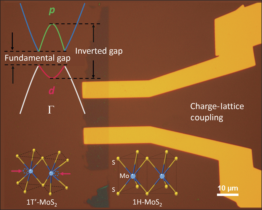
The different crystal structures of monolayer MoS2 and the observed tunable inverted gap and fundamental gap. Image provided by Xinmao Yin, Wenjing Zhang, Andrivo Rusydi, and Andrew T.S. Wee.
High-quality and large-area MoS2 monolayers were prepared by transferring a chemical vapor deposition grown MoS2 monolayer from a sapphire surface to gold thin films sputtered on Si/SiO2 substrates, with subsequent annealing. Furthermore, electrical transport was measured in MoS2 field-effect transistors by fabricating Ti/Au electrodes using standard electron-beam lithography, and subsequently transferring a mechanically exfoliated (MoS2) monolayer onto them to form a MoS2/Au interface.
Ju Li from the Massachusetts Institute of Technology, an author of the original theoretical study in Science that had predicted this result, regards this new study as convincing proof for tuning the topologically inverted energy gap in 2D-TMDs by annealing, thereby modulating the lattice strain and electron donation. He further said that this study provides an important practical means of controlling the inversion and opens up new avenues for topological quantum computing, optoelectronics, and spintronics with 2D materials.
