


I. INTRODUCTION
Silicon’s overwhelming technical importance has prompted numerous studies of its mechanical properties. Much has thus been written on its fracture behavior, which is subject to several complexities, e.g., fracture anisotropy, Reference Ebrahimi and Kalwani1–Reference Pérez and Gumbsch3 a brittle-to-ductile transition (BDT), Reference St. John4–Reference Gally and Argon7 initiation fracture toughness Reference Zhao, Bardel, Maynadier and Nelias8,Reference Buehler, Tang, van Duin and Goddard9 and associated environmental effects, Reference Gleizer and Sherman10 slow crack growth, Reference Fitzgerald, Iyer, Dauskardt and Kenny11 dynamic fracture and instabilities, Reference Sherman, Markovitz and Barkai12,Reference Cramer, Wanner and Gumbsch13 fractal fracture surface characteristics, Reference Tsai and Mecholsky14 or failure mechanisms specific to applications such as in lithium-ion batteries. Reference Shi, Song, Ross, Somorjai, Ritchie and Komvopoulos15 Moreover, its availability in virtually defect-free single-crystalline high-purity form has made silicon an oft-used model material for the general study of brittle fracture (despite the fact that its fracture characteristics are highly complex).
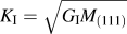
A bird’s eye view of the literature on the fracture of silicon reveals much scatter and inconsistency across the fracture toughness values reported. DelRio et al.
Reference DelRio, Cook and Boyce16
provide a critical, in-depth, survey of published measurements of silicon’s fracture toughness at room temperature. Focusing on silicon’s lowest energy planes, i.e., the (111) and the (110) planes, reported values cover the ranges ${K_{{\rm{Ic}}\left( {111} \right)}} = 0.65 - 1.7\;{\rm{MPa}}\,\sqrt {\rm{m}}$
and
${K_{{\rm{Ic}}\left( {111} \right)}} = 0.65 - 1.7\;{\rm{MPa}}\,\sqrt {\rm{m}}$
and ${K_{{\rm{Ic}}\left( {110} \right)}} = 0.7 - 2.5\;{\rm{MPa}}\,\sqrt {\rm{m}}$
; for comparison, values that have been predicted from bond energy and elastic moduli considerations are
${K_{{\rm{Ic}}\left( {110} \right)}} = 0.7 - 2.5\;{\rm{MPa}}\,\sqrt {\rm{m}}$
; for comparison, values that have been predicted from bond energy and elastic moduli considerations are ${K_{{\rm{Ic}}\left( {111} \right)}} = 0.72\;{\rm{MPa}}\,\sqrt {\rm{m}}$
and
${K_{{\rm{Ic}}\left( {111} \right)}} = 0.72\;{\rm{MPa}}\,\sqrt {\rm{m}}$
and ${K_{{\rm{Ic}}\left( {110} \right)}} = 0.73 - 0.82\;{\rm{MPa}}\,\sqrt {\rm{m}}$
.
Reference DelRio, Cook and Boyce16
Such a degree of scatter is impressive, particularly if one recalls that the surface energy is ultimately proportional to
${K_{{\rm{Ic}}\left( {110} \right)}} = 0.73 - 0.82\;{\rm{MPa}}\,\sqrt {\rm{m}}$
.
Reference DelRio, Cook and Boyce16
Such a degree of scatter is impressive, particularly if one recalls that the surface energy is ultimately proportional to $\mathop {{K_{{\rm{Ic}}}}}\nolimits^2$
. As discussed in sections C6–C8 of Ref. Reference DelRio, Cook and Boyce16, a number of studies must be excluded due to their lack of accuracy arising from basic flaws of methodology (notably data gleaned from nanoindentation cracking or from pre-notched specimens). Specifically, it is argued in Ref. Reference DelRio, Cook and Boyce16 that specimens in which a notch is introduced either by chemical etching or by ionbeam milling can lead to large overestimations of the fracture toughness in geometries where fracture is unstable and the notch is assimilated to a real crack. Among the remaining data, the lowest experimental values reported (i.e., 0.65
$\mathop {{K_{{\rm{Ic}}}}}\nolimits^2$
. As discussed in sections C6–C8 of Ref. Reference DelRio, Cook and Boyce16, a number of studies must be excluded due to their lack of accuracy arising from basic flaws of methodology (notably data gleaned from nanoindentation cracking or from pre-notched specimens). Specifically, it is argued in Ref. Reference DelRio, Cook and Boyce16 that specimens in which a notch is introduced either by chemical etching or by ionbeam milling can lead to large overestimations of the fracture toughness in geometries where fracture is unstable and the notch is assimilated to a real crack. Among the remaining data, the lowest experimental values reported (i.e., 0.65 ${\rm{MPa}}\,\sqrt {\rm{m}}$
Reference DelRio, Cook and Boyce16–Reference Jaccodine18
) were later re-analyzed yielding higher results,
Reference St. John4
thus narrowing the range to
${\rm{MPa}}\,\sqrt {\rm{m}}$
Reference DelRio, Cook and Boyce16–Reference Jaccodine18
) were later re-analyzed yielding higher results,
Reference St. John4
thus narrowing the range to ${K_{{\rm{Ic}}(111)}} = 0.83 - 1.0\;{\rm{MPa}}\,\sqrt {\rm{m}}$
or, using
${K_{{\rm{Ic}}(111)}} = 0.83 - 1.0\;{\rm{MPa}}\,\sqrt {\rm{m}}$
or, using ${K_{\rm{I}}} = \sqrt {{G_{\rm{I}}}{M_{(111)}}}$
with
${K_{\rm{I}}} = \sqrt {{G_{\rm{I}}}{M_{(111)}}}$
with ${M_{(111)}} = 178\;{\rm{GPa}}$
the effective modulus accounting for anisotropy,
Reference DelRio, Cook and Boyce16
${M_{(111)}} = 178\;{\rm{GPa}}$
the effective modulus accounting for anisotropy,
Reference DelRio, Cook and Boyce16 ${G_{{\rm{Ic}}(111)}} = 3.9 - 5.6\;{\rm{J/}}{{\rm{m}}^2}$
[to be compared with the predicted fracture energy
${G_{{\rm{Ic}}(111)}} = 3.9 - 5.6\;{\rm{J/}}{{\rm{m}}^2}$
[to be compared with the predicted fracture energy $2{\gamma _{(111)}} = 2.94\;{\rm{J/}}{{\rm{m}}^2}$
(Ref. Reference DelRio, Cook and Boyce16)].
$2{\gamma _{(111)}} = 2.94\;{\rm{J/}}{{\rm{m}}^2}$
(Ref. Reference DelRio, Cook and Boyce16)].
Adding to this complexity, the small scale testing community has provided interesting data and observations. Nakao et al. Reference Nakao, Ando, Shikida and Sato19 measured a BDT temperature as low as 65 °C using single-edge notched tensile specimens 45 µm wide and 4 µm thick with a 1–2 µm notch introduced by focused ion beam (FIB) milling; this value is in strong contrast with BDT temperatures documented for bulk silicon, which are around 600 °C Reference Ganchenkova and Nieminen20 (the exact value depends on the orientation and the strain rate Reference Samuels, Roberts and Hirsch5,Reference Hirsch and Roberts21 ). Also, it has been acknowledged that dislocation motion is enabled at room temperature in nanometre-scale silicon samples. Reference Gerberich, Michler, Mook, Ghisleni, Östlund, Stauffer and Ballarini22–Reference Gerberich, Stauffer, Beaber and Tymiak24 This has been observed in compression tests of nanoparticles less than 100 nm in diameter, Reference Gerberich, Mook, Perrey, Carter, Baskes, Mukherjee, Gidwani, Heberlein, McMurry and Girshick25–Reference Mook, Nowak, Perrey, Carter, Mukherjee, Girshick, McMurry and Gerberich27 during in situ TEM nanoindentation Reference Minor, Lilleodden, Jin, Stach, Chrzan and Morris28 or nanowire tension Reference Han, Zheng, Zhang, Zhang, Zhang and Wang29 tests, and in FIB-produced nanopillars of diameter below 400 nm. Reference Östlund, Rzepiejewska-Malyska, Leifer, Hale, Tang, Ballarini, Gerberich and Michler30 In nanopillars, a strong influence of the FIB in promoting dislocation activity has later been proven. Reference Wang, Xie, Ning and Shan31,Reference Wang, Zhang, Wang, Zhuang, Ma, Li and Shan32 Namely, it was shown that the FIB-introduced amorphous surface layer confining crystalline silicon first enhances incipient plasticity and then, as deformation progresses, leads to amorphization (followed by further deformation) of the crystalline silicon within the bulk of the pillars. Reference Wang, Zhang, Wang, Zhuang, Ma, Li and Shan32 Another potential concern regarding some of the studies cited above is the possible influence of the high energy electron beams used for in situ TEM tests on the mechanical response of silicon nano-sized samples, an effect that has been demonstrated in other materials Reference Zheng, Wang, Cheng, Yue, Han, Zhang, Shan, Mao, Ye, Yin and Ma33,Reference Zang, Bao, Webb and Li34 but found to be negligible in Si nanopillars by Wang et al., Reference Wang, Zhang, Wang, Zhuang, Ma, Li and Shan32 who measured the same response on 150 nm nanopillars tested with the beam on or with the beam off. Finally, it is interesting to note that there are also works that challenge the occurrence of plastic deformation in nanometre-sized silicon samples (none of them prepared with ion-milling nor pre-cracked): fully elastic behavior until fracture was observed on nanowires 100 nm in diameter tested in tension Reference Zhang, Tersoff, Xu, Chen, Zhang, Zhang, Yang, Lee, Tu, Li and Lu35 and on nanowires down to 20 nm in diameter tested in bending. Reference Stan, Krylyuk, Davydov, Levin and Cook36
Early TEM examinations Reference Lawn, Hockey and Wiederhorn37,Reference Tanaka, Higashida, Kishikawa and Morikawa38 have led to generally accept that silicon is an example of a perfectly brittle crystalline material at room temperature, i.e., featuring atomically sharp cracks and no dislocations around the crack tip. Later work by Langer et al. Reference Langer and Katzer39 showed, however, the emission of dislocations on a growing crack during an in situ bending test in the TEM at room temperature. While this observation might also have betrayed an influence of ion-milling (as mentioned above), the recent work by Adhika et al., Reference Adhika, Tanaka, Daio and Higashida40 on samples free of such potential artifacts, has shown dislocations at the tip of cracks in the {110} fracture plane produced by Vickers indentation at room temperature and examined post-mortem in the TEM. These dislocations induce a compressive stress state at the crack tip, which will cause crack tip shielding. Limited but finite crack tip plasticity in silicon has been proposed to explain the fact that measured critical strain energy release rates are normally higher than surface energies in many brittle and semibrittle materials, including silicon. Reference Gerberich, Mook, Carter and Ballarini41
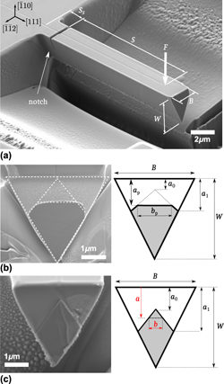
We present here an exploration of the fracture of silicon along its (111) plane by testing it at microscopic scale using FIB-produced microcantilever beams containing one of two kinds of notches: (i) the straight-through notch (STN)
Reference Di Maio and Roberts42–Reference Bohnert, Schmitt, Weygand, Kraft and Schwaiger52
or (ii) the chevron notch (CN).
Reference Bohnert, Schmitt, Weygand, Kraft and Schwaiger52–Reference Cui and Vinci55
While the STN test relies on the assumption that the notch accurately represents a real crack, the distinctive feature of the CN test is that it ensures that the fracture toughness is determined using a sharp crack because, as a consequence of its notch geometry, crack initiation is (in successful tests) followed by a stage of stable crack growth. As will be seen, the CN results are unfortunately highly erratic but data give evidence for extensions and arrests of a growing crack at varying driving forces in the $\left( {111} \right)\left[ {\bar 110} \right]$
fracture system. This observation implies that there are variations in the intrinsic fracture toughness of silicon along the path of a crack, and that this might be linked with the presence of limited room temperature dislocation activity at the crack tip in such samples.
$\left( {111} \right)\left[ {\bar 110} \right]$
fracture system. This observation implies that there are variations in the intrinsic fracture toughness of silicon along the path of a crack, and that this might be linked with the presence of limited room temperature dislocation activity at the crack tip in such samples.
II. MATERIALS AND METHODS
Microscopic cantilever beams of triangular cross-section were carved into the surface of a $\left( {\bar 110} \right)$
Czochralski silicon wafer slightly p-doped with B (resistivity 1–10 ohm cm) using FIB milling on a Zeiss™ NVision™ 40 (Oberkochen, Germany) SEM/FIB dual-beam system using 30 kV Ga+ ions. Currents ranged from 3 nA for the initial rough milling steps down to 700 pA for the final milling steps. Close to the root of each cantilever one of two types of notch was machined: either (i) a chevron notch (milled at ±30° from the top) or (ii) a STN (milled straight down from the top) was produced by FIB milling with a much lower current of 10 pA, chosen to minimize the notch thickness, Fig. 1. Specimens and the machined notches were oriented such as to probe the (111) fracture plane with a crack growing in the
$\left( {\bar 110} \right)$
Czochralski silicon wafer slightly p-doped with B (resistivity 1–10 ohm cm) using FIB milling on a Zeiss™ NVision™ 40 (Oberkochen, Germany) SEM/FIB dual-beam system using 30 kV Ga+ ions. Currents ranged from 3 nA for the initial rough milling steps down to 700 pA for the final milling steps. Close to the root of each cantilever one of two types of notch was machined: either (i) a chevron notch (milled at ±30° from the top) or (ii) a STN (milled straight down from the top) was produced by FIB milling with a much lower current of 10 pA, chosen to minimize the notch thickness, Fig. 1. Specimens and the machined notches were oriented such as to probe the (111) fracture plane with a crack growing in the $\left[ {\bar 110} \right]$
direction. Once prepared, samples were carefully checked in the SEM/FIB to ensure the absence of redeposited material along or around the notch.
$\left[ {\bar 110} \right]$
direction. Once prepared, samples were carefully checked in the SEM/FIB to ensure the absence of redeposited material along or around the notch.

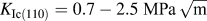
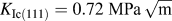
FIG. 1. (a) General geometry of triangular micro-cantilevers prepared by FIB milling single crystal silicon (110) wafer. (b) STN (Sample S4, Table I) and (c) chevron notch (Sample C2, Table I) fracture surfaces of tested cantilevers (shaded in gray on the right-hand sketches). STNs are FIB-milled perpendicular to the $\left( {\bar 110} \right)$
plane, which preferentially removes material near the edges of the notch front. To account for that, the geometry of these samples is approximated in calculations as being chevron-like with a static crack length a = a
p (see Sketch).
$\left( {\bar 110} \right)$
plane, which preferentially removes material near the edges of the notch front. To account for that, the geometry of these samples is approximated in calculations as being chevron-like with a static crack length a = a
p (see Sketch).
The micromechanical tests were conducted using a TI 950 TriboIndenter® (Hysitron® Corporation, Minneapolis, MN) nanoindentation apparatus, equipped with a cube-corner diamond tip, to apply the load and measure the load-point displacement. Each specimen was aligned to have the loading axis within ±0.5° of the normal to its top surface; this was achieved using the nanoindenter’s scanning probe microscope (SPM) capability and a two-axis goniometric tilt stage (Newport Corp., Irvine, CA) fixed on the positioning stage. The SPM was also used to aim the point of load application at the cantilever’s centreline close to its free end. The tests were conducted in the apparatus’s “load control” mode. The loading rate was set to 0.8 µN/s and kept at that value until fracture; note however that, as discussed below, the tests were not effectively run in an ideal but rather in an over-damped load control mode. At the end of a test, each sample was taken into the SEM to examine its fracture surface, measure the dimensions of the ligament, and identify the point of load application, which was revealed as an indent in the now-disconnected cantilever arm.
The most usual difficulty encountered in the use of CN specimens for the fracture testing of brittle materials (regardless of sample size) is that cracks can be difficult to initiate at the tip of the chevron notch. This leads to the frequent observation of rapid fracture at loads well above those that would be required to propagate the crack across the chevron-shaped ligament. This limitation was observed with the present microscopic silicon samples during preliminary tests of this work. To ease crack initiation at low applied loads and thus overcome the crack initiation problem encountered in early attempts (see Sec. IVB for details) the following procedure was used before the fracture test. In the SEM/FIB apparatus, after having produced a cantilever beam with a chevron notch using FIB-milling as described above, a micromanipulator tungsten needle (Kleindiek Nanotechnik GmbH, Reutlingen, Germany) was approached to the cantilever’s free end, welded to it with a small carbon deposit and moved cyclically up and down by a distance of roughly 0.5 µm 10 to 15 times, so as to produce slight, elastic bending of the chevron notched cantilever; Fig. S1 shows the process. This procedure induces concentrated cyclic strain in the material at the triangular ligament’s tip (a region composed of FIB-affected material). The needle was then detached from the cantilever by FIB milling the weld and the cantilever’s free end, which shortened the beam by a few micrometres, bringing it to its final geometry. The result of this initial “small chevron notch tip pre-fatigue” step in the sample preparation process was found to be that, when loading the beam during the fracture toughness test, cracking was initiated at applied loads low enough to enable subsequent stable growth of the crack across the chevron ligament.
The dimensions of all the samples tested in this work, which are defined in Fig. 1, are given in Table I. Based on that information, bespoke 3D finite element (FE) models were implemented in Abaqus/Standard™ 6.11 software (Dassault Systèmes, Providence, RI) to calculate the compliance calibration functions of CN and STN samples, in a similar way as was done in Refs. Reference Mueller, Pejchal, Žagar, Singh, Cantoni and Mortensen53 and Reference Žagar, Pejchal, Mueller, Michelet and Mortensen54 with the difference, however, that here the material’s elastic anisotropy is considered: single-crystalline silicon has a cubic-symmetry stiffness matrix with the three independent linear elastic constants c 11 = 166 GPa, c 12 = 64 GPa and c 44 = 80 GPa. Reference DelRio, Cook and Boyce16 The compliance dependence on crack length, C(a), in CN samples is obtained by first calculating a series of the compliance values C at increasing values of crack length a for each cantilever geometry [Fig. S6(a) symbols] and subsequently fitting those data with a polynomial function [Fig. S6(a), lines]. Note that in all stages of the work (in both calculations and data interpretation) the crack is assumed to be straight. The change of the compliance with respect to the crack length for each CN sample, dC/da, is then obtained by evaluating the derivative of the fitted polynomial.
TABLE I. Geometrical parameters of straight-through (S1–S4) and chevron (C1–C3) notched cantilevers, as defined in Fig. 1.

The released elastic strain energy rate G is finally calculated according to
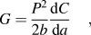 $$G = {{{P^2}} \over {2b}}{{{\rm{d}}C} \over {{\rm{d}}a}}\quad ,$$
where P is the load measured in the test, b is the width of the crack front (see below), and dC/da is the derivative of the compliance function (calculated using bespoke finite element modeling as explained above) evaluated, in the case of CN tests, at the crack length that is derived from the measured compliance, itself extracted from the slope of the line connecting each data point in the indentation-corrected load–displacement curve to the origin.
Because FIB milling of STNs causes removal of the material near the notch ends [Figs. 1(b) and S3], the geometry of the STN samples resembles that of the CN samples with a finite crack length a = a p [outlined with dashed line in Figs. 1(b) and S3]. Thus, the compliance calibration function of STN samples was calculated in a similar way as for CN specimens, with the difference that the change of the compliance with respect to the crack length in STN samples is evaluated by the finite difference approximation, i.e., dC/da = [C(a p + da) − C(a p)]/da where C(a p + da) and C(a p) are obtained from FE calculations with da = 1 nm. Scripts that aid in generating Abaqus chevron-notch FE models, used here to obtain the compliance calibration functions, are made freely available for download from the web site of our laboratory. 56
For CN samples, the crack front width b (assumed to be straight) is an increasing function of the crack length, i.e.,
 $$b = B\left( {1 - {a_1}/W} \right) \times \left( {a - {a_0}} \right)/\left( {{a_1} - {a_0}} \right)\quad .$$
For STN samples, the crack front width is a constant obtained simply by evaluating the expression for b of CN samples at a = a p. For simplicity, Eq. (1) can be contracted to G = P 2 g F(a), if we define the geometrical function g F(a) = 1/(2b) × dC/da (note that this is simply the dimensional counterpart in units of [N−1 m−1] of the geometrical function, F v(a/W), reported in Refs. Reference Mueller, Pejchal, Žagar, Singh, Cantoni and Mortensen53 and Reference Žagar, Pejchal, Mueller, Michelet and Mortensen54). Geometrical functions g F calculated for CN specimens of this work are given in the Supplementary Material, Fig. S6(b).
III. RESULTS
The load–displacement responses corrected for indentation of the STN or CN cantilever beams are shown, respectively, in Figs. 2 and 3. STN curves are linear until the point of sudden fracture, defined by a sudden large load drop and displacement jump (Fig. 2). Predictions of the finite element model were validated for all four STN samples in that the measured compliance and the calculated compliance match for all samples, Table II, where apparent silicon fracture toughness values computed by assimilating the notches to cracks are also listed.

FIG. 2. Force–displacement response of micro-cantilevers with STNs (STN Samples S1–S4, Table I). All data are corrected for additional displacement caused by tip indentation into the cantilevers.

FIG. 3. Force–displacement response of micro-cantilevers with chevron notch (CN Samples C1–C3, Table I). All data are corrected for displacements due to relative tip indentation into the cantilevers. Region of the response of chevron-notched cantilevers where the crack is growing is indicated with bold lines.
TABLE II. Experimentally measured fracture load P c and compliance C e, and calculated model compliance C m, geometrical function g F, critical released elastic energy rate G c and fracture toughness K Ic for micro-cantilevers with a STN.

With CN specimens (Fig. 3), loading curves are only linear up to a point where a first, small “pop-in” (load drop and displacement jump) is observed: this is the moment of crack initiation. During pop-ins, displacement of the sample is sudden and rapid; load–displacement data during those phases of the test are therefore not to be trusted, given that the indenter load control loop might not have had the capacity to follow the sample, leading to the possibility that there was temporary loss of contact during the rapid pop-in phase of the event. Thereafter, the curve stabilizes, and continues with a lower slope, betraying an increased compliance as a result of the pop-in event. With Samples C1 and C2 the curves present successive pop-in events appearing prior to the point of final, catastrophic fracture, which is characterized by a final large drop down to zero load.
The portion of the load–displacement curves that stretches between crack initiation and final fracture is indicated in bold for each CN sample in Fig. 3. The measured compliance as a function of the displacement in that region is plotted in the top row of Fig. 4. As seen, the compliance increases significantly with each pop-in in Samples C1 and C2, while it only increases slightly between pop-ins. Changes in compliance are signatures of crack growth; thus, pop-ins are sudden crack extensions followed by crack arrest and periods of crack growth at a much slower rate under increasing load. The bottom row of Fig. 4 shows how the strain energy release rate G (or stress intensity factor K I in the right-hand axis) varied during the crack growth process in each of Samples C1, C2, and C3; as seen, the data vary significantly from sample to sample.

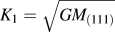
FIG. 4. (Top row) Linear elastic compliance C = u/P versus displacement u obtained from CN cantilever responses shown in Fig. 3 (only data indicated with a bold line are considered). (Bottom row) Calculated elastic strain energy release rate G versus measured displacement u. For convenience, right-hand scale corresponding to the stress intensity is indicated according to, ${K_1} = \sqrt {G{M_{(111)}}}$
, where the elastic fracture factor of SC Si for (111) plane M
(111) = 178 GPa.
Reference DelRio, Cook and Boyce16
The dotted line indicates the critical compliance that corresponds to the critical crack length of the chevron-notched geometry.
${K_1} = \sqrt {G{M_{(111)}}}$
, where the elastic fracture factor of SC Si for (111) plane M
(111) = 178 GPa.
Reference DelRio, Cook and Boyce16
The dotted line indicates the critical compliance that corresponds to the critical crack length of the chevron-notched geometry.
The fracture surfaces of all STN and CN specimens are globally flat, showing that the general crack propagation plane did not deviate significantly from (111); see Figs. 1(b)–1(c), S3 and S4. Besides the easily visible terrace-kink feature on Sample C2, in the fracture surfaces several tiny marks parallel or oblique to the expected crack front direction can be distinguished upon examination at high resolution (bottom row of Figs. S3 and S4).
Finally, we note that the justification for taking G = G I throughout this work comes out of the evaluation of the Mode II contribution to the total strain energy release rate G for the present specimen configurations (for details, see Supplementary Material). Results indicate that it reaches, in the worst case, only 5% of the total G value; hence, we deem it negligible. We also neglect the influence of potential beam twisting resulting from either off-centred loading or an off-centred position of the ligament at the notch. This is justified by the post-mortem observations in the SEM that, in all cases, the small indent left at the point of load application on the top surface of the post-test disconnected cantilevers was found to be within ∼50 nm of the cantilever centreline (Fig. S10), and the ligament at the notch was well-centred within ∼100 nm.
IV. DISCUSSION
A. Straight-through notched samples
As is known, using FIB-milled STN specimens to evaluate fracture toughness at a small scale is questionable; reasons for this are 3-fold: (i) assimilating a notch to a crack, given the finite notch-tip radius, Reference DelRio, Cook and Boyce16 (ii) the fact that the material itself at, and around, the crack tip is modified, to a higher or lesser extend depending on the material, after FIB-milling Reference Rubanov and Munroe57–Reference Rubanov59 (especially when the incident FIB is perpendicular to the surface, Reference Rubanov and Munroe57,Reference Rubanov59,Reference Roediger, Wanzenboeck, Waid, Hochleitner and Bertagnolli60 which is how STN samples are mostly produced; see also Sec. IV.C) and (iii) ion implantation, which can locally produce residual stresses that alter, to a remarkably large extent in some materials, Reference Norton, Falco, Young, Severs and Todd47 the effective stress field at the notch tip.
Here, measured critical strain energy release rate G Ic(111) values in STN Specimens S2–S4 are near ≈6 J/m2. This value comes close to the result of the pioneering work of Di Maio and Roberts Reference Di Maio and Roberts42 that constitutes, together with the present work, the only (to the best of our knowledge) fracture toughness measurement of the (111) fracture plane in silicon done at the microscopic scale. In Specimen S1, however, a value roughly twice as high was recorded (G Ic(111) = 12.7 J/m2), even though nothing particular is observed in this specimen with respect to the other three similar specimens (other than that it is marginally smaller in size). Overall, the STN results are about twice and four times, respectively, the theoretical fracture energy of Si along (111) planes: 2γ(111) = 2.94 J/m2 (Ref. Reference DelRio, Cook and Boyce16) and fall slightly above the range of experimental values reported in literature for the (111) fracture plane in silicon (omitting measurements that used either indentation or ionbeam-notched techniques, see Sec. I and Ref. Reference DelRio, Cook and Boyce16).
This overestimation seems to be in contrast with the work of Jaya et al.
Reference Jaya, Kirchlechner and Dehm48
on the (110) fracture plane in silicon; these authors reported, using notched microscopic specimens, measured fracture toughness values that fall within the expected range for that plane (note that there is a typo in the notch orientation in Ref. Reference Jaya, Kirchlechner and Dehm48, which should read “ $\left( {\bar 110} \right)\left[ {001} \right]$
”
Reference Jaya61
). Note, however, that in an earlier contribution the fracture toughness values gleaned using similar notched microscopic specimens in that same plane were far higher.
Reference Jaya and Jayaram62
Also, in a separate work, high fracture toughness values were obtained in microscopic STN clamped silicon beams when probing a (110) plane,
Reference Hintsala, Bhowmick, Yueyue, Ballarini, Asif and Gerberich63
prompting the authors to introduce a correction factor to lower the fracture toughness closer to expected values.
$\left( {\bar 110} \right)\left[ {001} \right]$
”
Reference Jaya61
). Note, however, that in an earlier contribution the fracture toughness values gleaned using similar notched microscopic specimens in that same plane were far higher.
Reference Jaya and Jayaram62
Also, in a separate work, high fracture toughness values were obtained in microscopic STN clamped silicon beams when probing a (110) plane,
Reference Hintsala, Bhowmick, Yueyue, Ballarini, Asif and Gerberich63
prompting the authors to introduce a correction factor to lower the fracture toughness closer to expected values.
In summary, even though it seems that the concerns about the STN technique mentioned above do not always affect results to a large extent in silicon (e.g., Ref. Reference Jaya, Kirchlechner and Dehm48 and Samples S2–S4 in this work), the present data add to the pool of data suggesting that measurements of toughness in silicon using microscopic STN samples can lead to (large) overestimations.
B. Crack initiation in microscopic chevron-notched specimens
The ability to initiate the crack at an early stage of the test and to subsequently grow it in a stable fashion are key requirements for a valid CN test. Early attempts by ourselves to perform microscopic CN fracture toughness tests on $\left( {\bar 110} \right)$
and on (111) silicon wafers oriented to probe the
$\left( {\bar 110} \right)$
and on (111) silicon wafers oriented to probe the $\left( {111} \right)[\bar 110]$
or the
$\left( {111} \right)[\bar 110]$
or the $\left( {\bar 110} \right)\left[ {111} \right]$
fracture systems were unsuccessful in that crack initiation was not followed by crack growth and thus occurred at a load higher than the critical load (which in CN samples is defined by their geometry and the material’s fracture toughness). As a result, complete fracture of the samples occurred as soon as a crack was nucleated, rendering the tests invalid.
$\left( {\bar 110} \right)\left[ {111} \right]$
fracture systems were unsuccessful in that crack initiation was not followed by crack growth and thus occurred at a load higher than the critical load (which in CN samples is defined by their geometry and the material’s fracture toughness). As a result, complete fracture of the samples occurred as soon as a crack was nucleated, rendering the tests invalid.
This crack initiation problem was not encountered when nanocrystalline alumina or amorphous fused quartz were tested in the same way. Reference Mueller, Pejchal, Žagar, Singh, Cantoni and Mortensen53,Reference Žagar, Pejchal, Mueller, Michelet and Mortensen54 Reasons why it is present with single-crystalline silicon are unclear. One possible explanation is that difficulty in initiating a crack in silicon results from the nature and/or extent of FIB damage to the machined surface, as the tip of the triangular ligament is a spot highly exposed to the FIB. Amorphization of the silicon at that spot is to be expected Reference Rubanov and Munroe57–Reference Rubanov59 and FIB damage in the form of gallium implantation is clearly present; we observed the formation of gallium droplets at the notch of Specimen C2 after performing the initial pre-fatigue step, see Fig. S5 (these droplets were subsequently removed using the FIB before testing the sample). Residual stresses caused by gallium implantation could also play a role, this effect being likely strongly material-specific; for example, Norton et al. Reference Norton, Falco, Young, Severs and Todd47 estimated the residual stress at the notch of a microscopic STN specimen in alumina to be in the range 12–15 GPa in compression over a depth of 20 nm. In one of our early trials on silicon, we introduced a CN sample into a furnace at 500 °C for 30 min under vacuum before the mechanical test (in an attempt to test whether residual stresses were the cause for the difficulty in crack initiation). Here too we found that a droplet had exuded at the notch after the heat-treatment (Fig. S7; in the subsequent mechanical test this sample did not show stable crack growth and was therefore discarded, as was the use of heat-treatment prior to testing). The difficulty in initiating a crack at the tip of the chevron notch in silicon, and/or the relative ease found in doing so in silica or nano-crystalline alumina, Reference Mueller, Pejchal, Žagar, Singh, Cantoni and Mortensen53,Reference Žagar, Pejchal, Mueller, Michelet and Mortensen54 might thus be related to differences in the nature and level of FIB-induced microdamage from one material to the other. Reference Norton, Falco, Young, Severs and Todd47
We therefore explored several approaches to ease crack initiation in silicon CN specimens; among these, the only successful procedure was the “chevron notch tip pre-fatigue” process described above, in Sec. II. This procedure enabled the production of CN samples that could initiate stable cracks; however, operationally it is not trivial. Half of the cantilevers (four other samples than those tested) were fatally damaged in the process and had to be discarded. Furthermore, its effects are not fully understood (e.g., it might be that the cycling caused migration of implanted Ga atoms). This said, this preparation step was successful in that it did promote crack initiation at low applied loads in three (Samples C1–C3) out of the four specimens that had survived the preparation and pre-fatigue procedure.
What remains unclear is whether the process produces a (tiny) pre-crack or a different effect at the apex of the chevron notch. In observing the notch at high magnification before and after the process on Sample C2, a pre-crack may arguably be recognized (see Fig. S2); however, fully clear images of the notches could not be produced and hence we cannot provide a firm conclusion. Measured initial compliances and those calculated via FE match well in all three samples (see Table II), indicating that, if a pre-crack was present, it was sufficiently small to have an undetectable effect on the mechanical response of the beam and hence on the interpretation of the test.
C. Crack growth and fracture toughness
In a perfectly load-controlled chevron-notch fracture toughness test the geometry alone defines a specific crack length up to which a crack grows stably, and beyond which the sample fractures completely and suddenly, regardless of the material as long as its fracture toughness is constant. The point of instability is defined by the crack location at which the stress intensity factor has ceased to decrease with increasing crack length. In other words, the critical crack length, a c, is at the minimum of the function g F(a), itself computed from a compliance calibration procedure.
The test data for the silicon CN samples of this work, however, show deviations from this expected behavior. Namely, Samples C1 and C2 show that stable crack growth occurred also beyond the critical point at a > a c (see Fig. 4, where dotted lines indicate the compliance corresponding to the critical crack lengths) and that instability was reached at a lower load after passing the maximum value (Fig. 3). Moreover, Samples C1 and C2 also feature several pop-ins, which are indications of sudden crack extension followed by crack arrest. Close examination of the load as a function of time in these tests reveals that after each pop-in, the load immediately dropped and the set point in load was re-sought very slowly by the nanoindenter, indicating an over-damped machine response. Such sluggish load-control most likely allowed the crack to immediately lose its driving force after a pop-in and hence to arrest, such that, due to the imperfect load control, the present tests have characteristics of displacement-controlled tests. Now, as seen in Fig. 4 bottom row, neither the values of G at which the crack suddenly extends nor the G values at which the crack arrests are the same across successive pop-ins; rather, values are scattered over the range G Ic(111) ≈ 5 − 7.7 J/m2 (excluding the first crack extension of Sample C1 at 10.8 J/m2). These values are about twice the theoretical fracture energy of (111), 2γ(111) = 2.94 J/m2. Reference DelRio, Cook and Boyce16
The response of Sample C3 is altogether different. Here, other than at crack initiation, there is no succession of jump-like crack advances (Fig. 3); rather, the load and the associated apparent compliance increase continuously after crack initiation [Fig. 4(c) top row; this can also be seen directly on Fig. 3 using a ruler]. This increase in compliance can be interpreted in two possible ways. In the first interpretation, the compliance increase is attributed to stable crack growth, which progresses smoothly at a slow rate. The corresponding variation in strain energy release rate is over the range G Ic(111) ≈ 2.5 − 10.3 J/m2, ending with the latter value before the onset of rapid crack growth [Fig. 4(c) bottom row]. In a second interpretation of the C3 test, the apparent change in compliance is caused by drift in the displacement measurement (note that the drift rate is assessed prior to loading but its instantaneous value during a test is unknown). One can then evaluate the fracture toughness using the crack length calculated from the compliance right after the crack was initiated [Fig. 4(c)] and the measured forces corresponding to the initial crack arrest and to the final fracture events; this gives G Ic(111) ≈ 2.5 J/m2 and G Ic(111) ≈ 10.7 J/m2, respectively. As seen, regardless of whether stable crack growth took place or not in Sample C3 (after crack initiation), one obtains similar extreme values of G Ic(111); the reason for this is the weak dependence of g F with crack length near the minimum of g F in this specimen [see Fig. S6(b)]. We note in passing that the toughness value at crack arrest is close to 2γ(111).
Several studies have documented that the thickness of the amorphous layer on a side-wall (a wall parallel to the ion beam) produced by milling with a 30 kV Ga+ FIB is in the range 20–30 nm at saturation Reference Rubanov and Munroe57–Reference Rubanov59 ; this is what can be expected at the edges of the triangular ligament in the CN specimens tested in this work. Hence, except at the beginning of stable crack propagation, the proportion of damaged material along the crack front is small and becomes even smaller as the crack advances [because b increases linearly with a, see Fig. 1 and Eq. (2)]. The amorphous FIB-induced damage layer is thus not expected to pollute toughness measurements produced by a developed crack in a CN specimen. This is contrary to STN specimens, which probe the onset of propagation of a notch made of FIB-milled material, furthermore known to be thicker since in milling STN notches the ion beam is applied perpendicularly to the silicon (in this case the amorphous layer is ∼60 nm, Reference Rubanov and Munroe57,Reference Rubanov59 and the silicon structure can actually be affected down to a depth of 230 nm Reference Roediger, Wanzenboeck, Waid, Hochleitner and Bertagnolli60 ).
Summing up, we find that, also with the CN geometry and despite the expectation that this test is unaffected by FIB-damage, erratic values, well above the expected value of 2γ(111) = 2.94 J/m2 (Ref. Reference DelRio, Cook and Boyce16) are measured, with the exception of values at crack arrest in Specimen C3. Also, we note that the apparent fracture toughness values measured using CN samples are comparable to the values obtained from STN samples.
The finding that a growing crack in the (111) plane can propagate at a certain apparent critical stress intensity value and then arrest at a lower value, both values being higher than 2γ(111), is in line with results reported by St. John, Reference St. John4 where similar behavior and G Ic ranging from ∼4.6 to ∼5.4 J/m2 for Si in the same fracture system as in this work were measured at room temperature and also at −196 °C using much larger (millimetre-wide) double cantilever specimens in displacement-controlled testing. Reference St. John4 Thus, it is unlikely that the erratic crack growth leading to the scatter in fracture toughness was a consequence of the small sample size or a result of FIB damage. The possibility that the “small chevron notch pre-fatigue” preparation step introduces extensive plastic deformation into the material through which the crack grows during the test was evaluated using finite element analysis (for details, refer to Supplementary Material). Results show that extensive plasticity is very unlikely in the great majority of the ligament, with the exception being the very tip of the triangular ligament, where stress might be high enough to introduce some dislocations, which might have traveled some distance into the specimen (particularly if a pre-crack was created in the pre-fatigue process).
A likely explanation for the erratic response is, therefore, that it resulted from the fact that, in both Ref. Reference St. John4 and the present work, Si toughness measurements were produced using growing cracks, resulting in some, limited but finite, amount of dislocation emission and subsequent interaction with growing cracks. It was recently observed by TEM that dislocations are emitted at the tip of sharp cracks grown by microindentation in Si at room temperature Reference Adhika, Tanaka, Daio and Higashida40 (a phenomenon that was also suggested to hold for many brittle materials in Ref. Reference Gerberich, Mook, Carter and Ballarini41). It is thus possible that, as was also suggested in Ref. Reference St. John4, the emission of dislocations at the tip of growing cracks, and the ensuing finite and variable crack tip shielding, cause a departure in measured toughness values upward of the expected value for the onset of the propagation of a pristine crack.
Specifically, if we assume in a simple back-of-the-envelope calculation that advancing a crack in silicon will cause the nucleation of a new dislocation every time a increases by ∆a, we can estimate that the increment ∆G c in the work of fracture that is linked to dislocation emission is roughly µb 2/(∆a). With µ taken equal to the shear modulus of polycrystalline silicon (64.9 GPa) and b the dislocation Burgers vector (0.383 nm), Reference Kubin64 we can solve for the value ∆a needed to account for the difference between the theoretical fracture toughness value in silicon [≈3 J/m2 for (111)] and the values measured here (which fluctuate around 6 J/m2). We arrive at ∆a ≈ 3 nm, which is close to the distance measured between dislocations that were observed just ahead of a crack tip produced at room temperature in silicon and observed in Ref. Reference Adhika, Tanaka, Daio and Higashida40.
We thus propose that the tips of growing cracks in present samples emit stochastically a few dislocations and encounter previously emitted dislocations along the crack path, causing in the process variations in the apparent toughness linked with the number, nature, and orientation of the dislocations involved in those events. This could explain the observed variable excess in critical strain energy release rate that is required for the propagation of cracks in (111) silicon over and above the Griffith value 2γ(111) = 2.94 J/m2. One question this interpretation would raise is whether or not the FIB-affected layer of material at the edges of the ligament (and thus at the borders of the crack front) in the present CN tests plays a role in this process, by enhancing the level of dislocation activity, similarly to what was identified in FIB-produced silicon nanopillars. Reference Wang, Xie, Ning and Shan31
V. CONCLUSION
The fracture toughness of silicon at room temperature was probed at the microscopic scale using triangular cantilever beams with either straight-through (STN) or chevron (CN) notches along the (111) fracture plane with a $\left[ {\bar 110} \right]$
crack growth direction. CN tests reveal crack extension and arrest together with a jerky evolution of the fracture toughness during crack growth of a (short) crack. The mechanism responsible for this is at present undetermined; a strong candidate is stochastic crack tip dislocation activity producing crack tip shielding, which can also account for the fact that measured fracture toughness values (both here and in practically every study in literature) exceed the theoretical fracture energy 2γ(111). A second conclusion of this work is that the microscopic CN test, which promotes stable crack growth and is hence free from the artifacts of the STN test (and might be used in a far more extensive testing program aiming to generate statistically significant data on the stochastics of growing cracks in silicon), has in single-crystalline silicon crack initiation issues that make it inconvenient for this particular material.
$\left[ {\bar 110} \right]$
crack growth direction. CN tests reveal crack extension and arrest together with a jerky evolution of the fracture toughness during crack growth of a (short) crack. The mechanism responsible for this is at present undetermined; a strong candidate is stochastic crack tip dislocation activity producing crack tip shielding, which can also account for the fact that measured fracture toughness values (both here and in practically every study in literature) exceed the theoretical fracture energy 2γ(111). A second conclusion of this work is that the microscopic CN test, which promotes stable crack growth and is hence free from the artifacts of the STN test (and might be used in a far more extensive testing program aiming to generate statistically significant data on the stochastics of growing cracks in silicon), has in single-crystalline silicon crack initiation issues that make it inconvenient for this particular material.
Supplementary Material
To view supplementary material for this article, please visit https://doi.org/10.1557/jmr.2017.238.
ACKNOWLEDGMENTS
This research was funded by the European Research Council under the European Union’s Seventh Framework Program (FP/2007–2013)/ERC Advanced Grant Agreement No. 291085. Scanning electron microscopy and focused ion beam milling were performed at the Interdisciplinary Center of Electron Microscopy at the Ecole Polytechnique Fédérale de Lausanne (CIME-EPFL).


 Open access