Introduction
Magnesium is the commonly used impurity for p-type doping of gallium nitride (GaN) and it can be introduced into the lattice during chemical vapor deposition (CVD) of GaN layers in an easy way [Reference Ambacher1]. Sufficient p-type activation of the GaN:Mg-layers is reached after a subsequent annealing step at around 800 °C. These p-type GaN-layers are successfully used for the fabrication of “blue” optoelectronic devices. However, the use of GaN is limited to such devices, because the growth process can result only into layered structures. The realization of lateral doped structures of GaN is therefore highly desirable in order to produce GaN based integrated microelectronics.
Lateral doping of semiconductors can be achieved by either in-diffusion or ion implantation of dopants through a structured mask. The diffusion method can be excluded in the case of GaN due to the fact that the diffusion of impurities in GaN starts at very high temperatures where the decomposition of the GaN surface/samples is already completed [Reference King, Barnak, Bremser, Tracy, Ronning, Davis and Nemanich2-Reference Vartuli, Pearton, Abernathy, MacKenzie, Lambers, Zolper and Vac3]. This early decomposition of the GaN surface at about 850 °C also hampers the success of ion implantation doping of GaN [Reference Zolper4]. The advantages of ion implantation (control of lateral and depth distributions, all elements are available) are compromised by the introduced radiation damage which has to be removed via annealing treatments. Annealing temperatures (TA) of about 1300 °C for more than 5 minutes are necessary for GaN to fulfil the rule of thumb claiming that implanted semiconductors should be annealed up to 2/3 of the melting point for satisfying electrical activation [Reference Ambacher1,Reference Edgar5,Reference Zolper, Pearton, Williams, Tan, Karlicek and Stall6]. Several special annealing procedures for temperatures above 900 °C have been investigated with limited success: rapid thermal annealing (RTA) [Reference Tan, Williams, Zou, Cockayne, Pearton, Zolper and Stall7,Reference Strite, Epperlein, Dommann, Rockett and Broom8], annealing under N2-overpressure [Reference Strite, Pelzmann, Suski, Leszczynski, Jun, Rockett, Kamp and Ebeling9], or the usage of N2, NH3 or atomic N fluxes, respectively [Reference Zolper, Han, Biefeld, Deusen, Wampler, Pearton, Williams, Tan, Karlicek and Stall10,Reference Ronning, Linthicum, Carlson, Hartlieb, Thomson, Gehrke and Davis11]. Polycrystalline, sputter deposited AlN cap layers were also used to protect decomposition during annealing. However, depending on the crystalline quality of the sputtered AlN, good results were obtained only for some selected samples [Reference Zolper, Pearton, Williams, Tan, Karlicek and Stall6,Reference Zolper, Han, Biefeld, Deusen, Wampler, Pearton, Williams, Tan, Karlicek and Stall10].
In this article we present results on the basis of an improved annealing technique. Instead of polycrystalline AlN-cap layers, we used thin AlN layers epitaxially grown on top of GaN-samples to protect the GaN surface from decomposition during annealing after the ion implantation of Mg. Magnesium was used because of its known behavior in GaN and the well known corresponding PL signatures.
Experimental
One-to-two µm thick epitaxial, monocrystalline and nominally undoped GaN films were grown on on-axis n-type, Si-face α(6H)-SiC(0001) substrates at 1000 °C and 45 Torr using a vertical, cold-wall, RF inductively heated MOVPE deposition system [Reference Weeks, Bremser, Ailey, Carlson, Perry and Davis12]. High-temperature (1100 °C) mono-crystalline AlN layers were deposited prior (100 nm) and following (30 nm) to the GaN growth. Deposition was performed using triethylaluminum (TEA) and triethylgallium (TEG) in combination with 1.5 SLM of ammonia (NH3) and 3 SLM of H2 diluent.
Magnesium was implanted with ion energies of 60 keV or 120 keV at room temperature. TRIM simulations gave a mean ion range of 70 nm (FWHM = 40 nm) and 127 nm (FWHM = 101 nm), respectively, for the two energies [Reference Ziegler, Biersack and Littmark13]. Thus, the implanted magnesium ions penetrated the AlN-cap layer in both cases, which was also experimentally checked and confirmed by SIMS measurements. The total implantation dose ranged between 1013 cm−2 and 1015 cm−2.
All implanted samples were annealed under vacuum (< 1.104 mbar) up to temperatures of 1300 °C for 10-30 minutes. The AlN cap layer inhibited surface decomposition of the GaN sample. Photoluminescence measurements (PL) were performed after each annealing step at low temperatures by exciting the GaN samples with a He-Cd laser (3.81 eV). The AlN-cap layer was removed by dry etching in an ICP plasma (300 W, bias: 10 V, 30 sec.) [Reference Smith, Wolden, Bremser, Hanser, Davis and Lampert14]. Hall measurements were done in Van-der-Pauw geometry after the deposition of Pd(50 nm)-Au(100nm) contacts at a rate of 0.1-0.2 nm/s and 6.10−6 mbar.
Results and Discussion
The low temperature PL spectra of Mg-implanted GaN with a dose of 1.1013 cm−2 are summarized in figure 1 as a function of annealing temperature and time. No PL lines were observed directly after ion implantation, which indicates a highly disturbed GaN lattice. This behavior was, of course, also observed for the higher implantation doses used in this study. The high defect density introduced into the crystal by the ion implantation process leads to non-radiative recombinations of the excited electrons with holes; thus, no luminescence is visible.

Figure 1. Photoluminescence spectra of GaN. The spectra were recorded in the situations: (a) as-implanted with Mg, and (b-d) after annealing to several temperatures for different times. The implantation energy was 60 keV and the implantation dose 1.1013 cm−2
Intense PL lines have been detected after annealing the Mg implanted GaN sample at a temperature of 1200 °C for 11 minutes (see figure 1(b)). However, the intensity of the band edge luminescence is still about 2-3 orders of magnitude lower in comparison to asgrown, unimplanted GaN samples. This luminescence line at 3.467 eV (commonly labeled as I2) originates from recombinations of excitons bound to shallow donors. The LO-phonon replica of this line at about 3.35 eV could not be observed in the implanted sample an nealed at 1200 °C for 11 minutes. However, it was observed as a shoulder after annealing at 1250 °C for 30 minutes and the PL intensity of the excitons also increased. A further increase of this I2-line took place after the 1300 °C annealing step for 10 minutes, as shown in Figure 1. This indicates that the implanted sample has been recovered to a large extent.
The luminescence peak, which appeared at 3.25 eV after the high temperature annealing steps, is related to donor acceptor pair (DAP) transitions involving Mg acceptors. This line with its LO-phonon replicas is commonly seen in GaN samples doped during growth with Mg showing p-type activation [Reference Oh, Park and Park15]. Therefore, we can conclude that optical activation of the implanted Mg atoms was reached. After the 1300 °C annealing step a further increase of the intensity took place and the optical activation seems to be almost complete, because the intensity of the 3.25 eV line with its phonon replicas is in the same order of PL-lines observed in GaN:Mg samples with an Mg concentration of about 1017−18 cm−3. This concentration corresponds well to the peak concentration of Mg atoms in the implanted region. Since we have never observed the PL-line at 3.25 eV after implantation of Be, Li, Si, Ge, In and Er into GaN [Reference Ronning, Linthicum, Carlson, Hartlieb, Thomson, Gehrke and Davis11,Reference Dalmer, Restle, Stötzler, Vetter, Hofsäss, Bremser, Ronning and Davis16,Reference Carlson, Ronning and Davis17], these observations prove that the line at 3.25 eV is only related to the implanted Mg acceptors, which is in agreement with Ref. [Reference Pong, Pan, Teng, Chi, Li, Lee and Lee18]. However, there is still a high intensity of the yellow PL-band observable between 2.0 and 2.6 eV in figure 1 after the 1300 °C annealing step, which indicates that remaining implantation defects are still present.
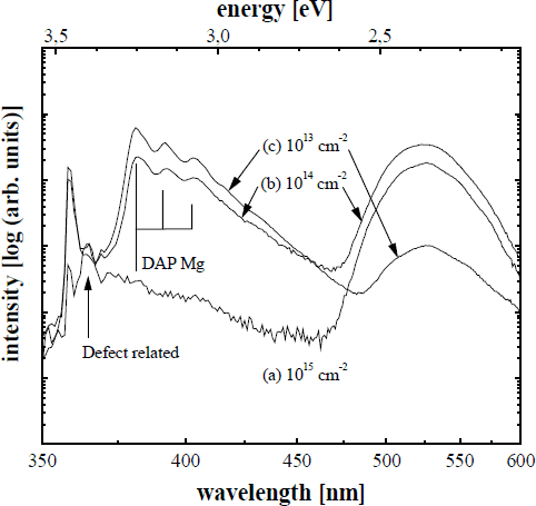
The low temperature PL-spectra of Mg implanted GaN samples annealed at 1250 °C for 30 minutes are shown in figure 2 as a function of the implantation dose. For comparison, the same scales of figure 1 were used in figure 2. The spectrum of the implanted sample with 1013 cm−2 Mg ions was already described above. With increasing implantation dose the Mg related DAP transition decreases, and finally the GaN samples implanted with a dose of 1015 cm−2 show no PL-transitions. One would not expect such a behavior, which was also observed after the 1300 °C annealing step, in completely recovered GaN:Mg samples. Therefore, an amount of residual defects, which strongly depends on the implantation dose, is still present in the annealed samples. This is supported by the fact that the behavior of the intensity of the yellow band is opposite to the behavior of the DAP transitions and therefore much higher in the GaN:Mg samples implanted with the higher implantation dose (see figure 2). Furthermore, the intensity of the band edge PL of the 1015 cm−2 GaN:Mg is suppressed by two orders of magnitude and an additional PL-line appears at 3.40 eV. This line is most likely related to defects created during the implantation procedure, as this line was also observed with varying intensities after implantation of Be, Li, Si, Ge, In and Er [Reference Ronning, Linthicum, Carlson, Hartlieb, Thomson, Gehrke and Davis11,Reference Carlson, Ronning and Davis17]. We believe that this line is produced by nitrogen or gallium vacancies due to acceptor or donor bound excitons, because it appears also in unimplanted GaN samples depending on the growth conditions.

Figure 2. Photoluminescence spectra measured at low temperature of GaN as a function of the Mg implantation dose. (a) 1015 cm−2, (b) 1014 cm−2, and (c) 1013 cm−2. The annealing was performed at 1250 °C for 30 minutes under vacuum and the implantation energy was set to 60 keV.
Finally, we want to compare PL-spectra obtained from GaN:Mg samples implanted with different ion energies. Figure 3 shows the PL spectra of two GaN samples annealed at 1250 °C for 30 minutes and implanted with a dose of 1013 cm−2 and an ion energy of 60 and 120 keV, respectively. The luminescence intensity of the 120 keV implanted GaN is at almost all wavelengths about one order of magnitude higher. This is again opposite to the expected behavior, because the higher implantation energy yields to a larger spatial distribution of the implanted Mg. The peak concentration is approximately a factor 2 lower compared to the 60 keV implanted sample and the DAP transitions are more intense. This can be explained by the fact that the introduced damage is also distributed over a larger volume and less implantation defects remain after the annealing.

Figure 3. Photoluminescence spectra measured at low temperature of GaN as a function of implantation energy. (a) 60 keV, and (b) 120 keV. The annealing was performed at 1250 °C for 30 minutes under vacuum and the implantation dose was 1013 cm−2.
Electrical measurements were performed after removing the AlN-cap by dry etching in an ICP plasma (300 W, bias: 10 V, 30 sec.) [Reference Smith, Wolden, Bremser, Hanser, Davis and Lampert14] and the deposition of Pd/Au contacts. The contacts showed ohmic behavior over a range of +/− 5 V, which is an important prerequisite for Hall effect measurements in Van-der-Pauw geometry [Reference van der Pauw19,Reference Sze20]. First, we want to notice that an electrical signal was only measurable in the Mg implanted GaN samples, which were annealed above a temperature of 1250 °C for more than 30 minutes. For lower annealing temperatures the GaN samples were too resistive (> 1010 Ω). The electrical measurements are summarized in table I.
Table I. Results of Hall measurements on Mg-implanted GaN samples.

In some cases the sign of the major charge carriers was not clear, because in several repeated measurements n- or p-type was measured. These measurements are indicated in the table I with n/p. This already indicates that the holes generated by the Mg acceptors are compensated by electrons. We assume that these donors are either due to remaining implantation defects or due to native donors from the as-grown GaN-samples. For comparison: the as-grown samples showed sheet concentrations of 1.5.1013 cm−2, which is comparable with the introduced Mg acceptors for the low implantation doses used. Furthermore, we observed a decrease of the sheet resistance, sheet carrier concentration and mobility for the higher implanted doses, which is definitively due to the remaining implantation defects (see PL-results).
Conclusions
Single crystalline (0001) GaN layers, capped with a thin epitaxial aluminum nitride layer, were implanted with magnesium and subsequently annealed within the range of 1150-1300 °C for 10-60 minutes in vacuum. PL measurements showed the typical DAP transition at 3.25 eV after annealing at high temperatures, which is related to optically active Mg acceptors in GaN. For low doses, high ion energies and high annealing temperatures the PL spectra seems to be completely recovered; however, this is not the case, as shown for higher implantation doses, lower ion energies and lower annealing temperatures. Therefore, the electrical measurements showed no p-type behavior of the GaN samples due to the compensation of the Mg acceptors with native or implantation n-type defects. In order to reach electrical activation higher annealing temperatures and annealing times should be necessary. For such experiments better vacuum conditions during the annealing must be realized, because beyond 1300 °C the AlN-cap starts to oxidize in the presence of even low partial pressures of oxygen.
Acknowledgements
The work at NCSU was supported by the Office of Naval Research via contract N00014-96-1-0765 monitored by Mr. Max Yoder. R.F. Davis was supported in part by the Kobe Steel, Ltd. Professorship.