

Bruker Nano Surfaces and Metrology
Tel: 520-741-1044, ext. 1075
Email: Productinfo@bruker.com

Hysitron PI 89 SEM PicoIndenter
APPLICATIONS: In-Situ Mechanical Experiments for SEM • Targeted Nanoindentation with EBSD • Heating up to 800°C • Nanoscratch • Data-Video Correlation
FEATURES: Hysitron PI 89 leverages the advanced imaging capabilities of SEM, FIBSEM, and PFIB, making it possible to perform quantitative nanomechanical testing while simultaneously imaging.

Hysitron PI 95 TEM PicoIndenter
APPLICATIONS: In-Situ Mechanical Experiments for TEM • Tensile Testing of Nanowires, Films, 2D Materials • Nanoscratch, Fatigue, Electrical, Heating • Data-Video Correlation
FEATURES: The only quantitative nanomechanical testing holder for TEM, enabling compression, tension, bending, scratch, and fatigue testing with simultaneous TEM observation of deformation behavior.
www.bruker.com/nanomechanical-testing

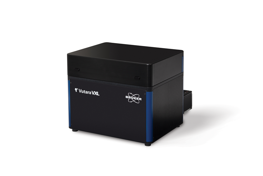
Vutara VXL Super-Resolution Microscope
APPLICATIONS: Video-Rate, Single-Molecule Localization • Quantitative Super-Resolution Analysis • Genomics Research • Developmental Biology • Cardiology
FEATURES: Vutara VXL's speed, imaging depth, and resolution deliver significant advantages over competing approaches, adding real-time quantitative analyses and including pair-correlation, co-location, cluster, and live-cell analysis.
Dimension XR SPM
APPLICATIONS: Quantitative Nanomechanical Analysis • Multi-Dimensional Nanoelectrical Characterization • Highest Resolution Scanning Electrochemical Imaging • Nanoscale Viscoelastic Analysis of Polymers
FEATURES: Packaged solutions for advanced, quantitative nanomechanical, nanoelectrical, and nanoelectrochemical research of materials and active nanoscale systems in air, fluid, electrical or chemically reactive environments.

Anasys nanoIR3 Spectrometer
APPLICATIONS: Hyperspectral NanoIR Spectroscopy Correlated to FTIR • Nanoscale Chemical Imaging • Complementary Tapping AFM-IR and s-SNOM 2D Materials Characterization • Semiconductor Failure Analysis
FEATURES: The nanoIR3 provides IR-based chemical imaging and mapping of chemical variations of sample. Point spectroscopy capabilities enable both spectroscopy and chemical imaging with a single source.

Ultima 2Pplus Multiphoton Microscope
APPLICATIONS: Neuroscience • Intravital Imaging • Optogenetics • Photoactivation and Photostimulation Experiments • In Vivo Imaging
FEATURES: Ultima 2Pplus delivers an ideal combination of flexibility, resolution, imaging depth and speed, allowing simultaneous imaging, stimulation and electrophysiology protocols with greater efficiency and effectivity.

Contour X 3D Optical Profilometer
APPLICATIONS: MEMS Characterization • Precision Machined Component Metrology • Tribology and Corrosion Analysis • High-Brightness LED Measurements • Opthalmic Characterization
FEATURES: The Contour X utilizes over four decades of white light interferometric (WLI) innovation to deliver production-ready automation, measurement-angle flexibility, outstanding imaging, and proven gauge-capable surface metrology.

Dimension IconIR Nanoscale Infrared Spectrometer
APPLICATIONS: Hyperspectral NanoIR Spectroscopy Correlated to FTIR • Correlative Chemical Imaging with Nanomechanical and Nanoelectrical Analyses • Resonance-Enhanced AFM-IR Characterization
FEATURES: IconIR combines world’s best large-sample AFM with nanoIR photothermal AFM-IR technology to establish new standards in chemical and material property mapping with sub-10nm chemical imaging resolution.

JPK NanoRacer High-Speed AFM
APPLICATIONS: Single-Molecule Investigations • Biochemistry Dynamics • High-Speed Nanoscale Biomedicine Research • Real-Time Molecular Biology
FEATURES: With an unprecedented imaging speed of 50 frames per second, NanoRacer sets a new AFM milestone to enable true real-time visualization of dynamic biological processes.

JPK NanoWizard 5 BioAFM
APPLICATIONS: Correlation with Optical Microscopy • Cell and Tissue Dynamics • Long-Term, Self-Regulating Experiments • High-Resolution, Quantitative Mechanobiology
FEATURES: Automated BioAFM that can be fully integrated with advanced optical microscopes to enable rapid, quantitative mechanical measurements and dynamics analysis of sub-molecular samples, cells, and tissues.

Bruker Nano Analytics
Tel: 1-800-234-9729
Email: info.bna@bruker.com
Electron Microscope Analyzers
PORTFOLIO: Energy-Dispersive X-ray Spectrometry (EDS) • Wavelength Dispersive X-ray Spectrometry (WDS) • Electron Backscatter Diffraction (EBSD) • Micro X-ray Fluorescence (Micro-XRF) on SEM • XFlash® Silicon Drift Detectors (SDD) for SEM and TEM
FEATURES: Bruker Nano Analytic's electron microscope analyzers QUANTAX EDS, QUANTAX WDS, QUANTAX EBSD and QUANTAX Micro-XRF on SEM offer unmatched comprehensive compositional and structural materials analysis.

Bruker Optics
Tel: 978-663-3660
Email: info.bopt.us@bruker.com
LUMOS II FTIR Microscope
APPLICATIONS: Failure Analysis • Particle & Surface Analysis • Life Science • Polymers & Plastics • Pharmaceuticals
FEATURES: The LUMOS II is a stand-alone FTIR microscope that excels in failure analysis, material research and particle analysis. It is compact, precise and features ultrafast chemical imaging by FPA technology.

HYPERION II
APPLICATIONS: Life Science/Cell • Imaging Pharmaceuticals • Forensics • Microplastics • Industrial R&D • Surface Analysis/Characterization
FEATURES: The HYPERION II Laser Imaging Microscope combines FT-IR and Infrared Laser Imaging (ILIM) microscopy in a single device, offering all three measurement modes: transmission, reflection, and ATR.

Deben
Tel: +44 (0) 1359 244 870 & +1 (201) 962 7222
Email: paulg@deben.co.uk

In-situ testing for microscopy
APPLICATIONS: • Microtest tensile and compression stages • Micro CT tensile, compression and torsion stages • STEM & BSE detectors for SEM • Centaurus scintillator CL and backscattered electron (BSE) detectors • SEM heating and cooling Peltier stages
FEATURES: Deben manufactures in-situ testing stages as well as innovative accessories for SEM, Optical, AFM, XRD and X-ray tomography.


QUADRO
APPLICATIONS: • Electron diffraction • 4D STEM • Strain Mapping • Ptychography • In-situ TEM
FEATURES: The QUADRO offers direct electron detection, region of interest feature, up to 18,000 frames/sec readout, noise-free electron counting, and the ideal DQE.
www.dectris.com/products/quadro/

Additional products…
ELA
APPLICATIONS: • Electron Energy Loss Spectroscopy (EELS) • Elemental mapping • 4D STEM
FEATURES: The ELA detector offers 4,500 full frames/sec and can go even faster for sub-areas without compromising the sensitivity and the high dynamic range. As a part of Gatan's integrated solution, DECTRIS ELA was recognized as Microscopy Today Innovation 2021.

SINGLA
APPLICATIONS: • Single-particle CryoEM • Electron tomography • MicroED • Small-molecule crystallography
FEATURES: The SINGLA allows for electron counting up to 107 electrons/pix/sec and a continuous readout at over 2,000 frames/sec.
www.dectris.com/products/singla/

DiATOME U.S.
Tel: 215-412-8390
Email: info@diatomeknives.com

DiATOME cryo Diamond Knives
APPLICATIONS: Available for wet or dry sectioning with a 25°, 35° or a 45° angle. Cutting edge sizes 1.5-4mm. Use for all low-temperature situations such as sectioning of cryo-protected specimens, frozen hydrated specimens, polymers, and rubber.
FEATURES: DiATOME...at the forefront of cryo innovation..

EMF, A Dynasil Company
Phone: +1-800-456-7070
Email: information@emf-corp.com
https://dysl.li/emf/microscopy

Metal-coated Microscope Test Slides
Applications: EMF's metal-coated microscope test slides are used in corrosion testing, scanning probe and Atomic Force Microscopy (AFM), Raman spectroscopy, microarrays, cell culture, biological and clinical research, analytical chemistry, electronics fabrication, industrial testing, and academic research in schools and universities.

Features: Slides are individually polished, cleaned, and inspected to maintain the highest standards. Substrates are pre-cleaned in a vacuum using an ion glow.
Gold: 1000Å of Au coated with 50Å binder layer of either Chromium or Titanium
Silver: Bare Ag at 1000Å
Copper: Cu ~500Å, conforms to ASTM D2671/IPC-TM-650
Aluminum: Bare Al at 1000Å

EDAX
Tel: (201) 529-4880
Email: info.edax@ametek.com

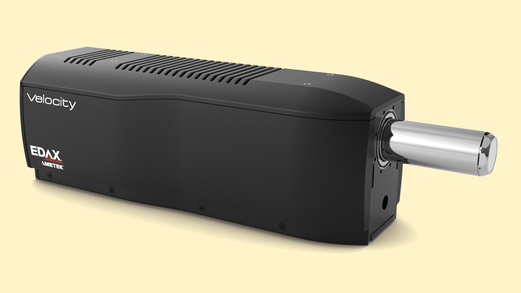
Velocity™ EBSD Camera Series
APPLICATIONS: Scanning Electron Microscopes (SEMs) • Electron Backscatter Diffraction (EBSD) • Simultaneous Energy Dispersive Spectroscopy (EDS)-EBSD Collection • Lower Symmetry, Multi-Phase, or Deformed Structures • In-situ and 3D EBSD Applications
FEATURES: Powered by a CMOS sensor, the Velocity combines fast acquisition with high sensitivity and low noise performance for optimal collection and data quality.
Electron Microscopy Sciences
Tel: 215-412-8400
E-mail: stacie@ems-secure.com

EMS-002 Cryo Workstation
The EMS-002 Cryo Workstation is a complete ultra rapid freezing system that captures rapid events and labile structures that are not seen in chemically fixed materials.

Etaluma, Inc.
Tel: 760-298-2355
Email: info@etaluma.com

Lumascope
APPLICATIONS: Cell Growth and Health • Immunofluorescence Assays • Spheroid/Organoid Growth monitoring • Protein Expression • Stemcell
FEATURES: Etaluma designs and manufactures high performance wide field fluorescence microscopy instruments for live-cell research and compact OEM assemblies for medical device partners.

Euclid Techlabs, LLC
Tel: (301) 637-0669
Email: info@euclidtechlabs.com

UltraFast Pulser
APPLICATIONS: • Affordable UTEM/SEM • Low Damage/Dose with Sensitive Samples • Picosecond Pump-Probe Stroboscopy • Sample Vibration Mitigation • EELS/Holography Compatibility
FEATURES: Field-retrofittable laser-free UEM pulser preserves native gun performance and offers adjustable 10ps-DC pulse width, Hz-10GHz repetition rate, and breakthrough stroboscopic/low-dose imaging rapidity.


Evactron® E50 E-TC Plasma De-Contaminator
APPLICATIONS: In-situ hydrocarbon removal • SEM/FIB large chamber cleaning • TKD/EBSD sample optimization • SEM sample and TEM holder cleaning • Accurate nanostructure characterization
FEATURES: External hollow cathode 50 watt plasma source with touchpad control, fast cleaning/pumpdown of large chambers, “POP” ignition at high vacuum - no venting needed.
https://evactron.com/evactron-e50-de-contaminators/

E16 SoftClean
APPLICATIONS: Clean sensitive FIB/SEM/TEM samples • Modify surface functional groups to improve hydrophilicity • High resolution TEM/STEM imaging and chemical mapping • Activate in-situ TEM and SEM chip surfaces • SEM and TEM sample storage
FEATURES: Remove hydrocarbon contamination from SEM samples and TEM holders, external energy-efficient hollow cathode 5-16 watt power to clean sensitive surfaces, uses air to generate a remote plasma, three ports for TEM holders and a top-loading chamber for SEM samples, includes an adjustable sample platform.
https://evactron.com/softclean/


X-Cite® Fluorescence Illumination Solutions
Email: x-cite@excelitas.com
APPLICATIONS: • Digital Pathology or Virtual Microscopy • Fluorescence in Situ Hybridization (FISH) • Fluorescence Resonance Energy Transfer (FRET) • Live Cell Imaging • Optogenetics • Photoactivation
FEATURES: X-Cite offers innovative and reliable fluorescence illumination solutions for researchers and OEM integrators, with the high power, control and stability required for their applications.
https://www.excelitas.com/product-category/x-cite-illuminators


Nicola G2/G2F ex situ lift out and micromanipulation system
APPLICATIONS: ex situ lift out • micromanipulation • particles, fibers, thin films • backside or plan view manipulation • FIB/SEM/TEM specimen preparation
FEATURES: EXpressLO™ patented grids and methods allow fast, easy, and flexible manipulation of FIB lift out specimens, fibers, particles, thin films, CNTs, and more.
https://www.expresslo.com/ex-situ-lift-out-systems.html

Additional products…
Praxis™ 3D Printed Samples
APPLICATIONS: ex situ lift out • in situ lift out • manipulation practice and training • reduce FIB costs for practice and training • access to an array of many samples
FEATURES: The patented Praxis™ 3D printed specimens can be used for EXLO or INLO methods, for training, practice, and educational purposes.
https://www.expresslo.com/praxis-.html

EXpressLO-Z™ Grids
APPLICATIONS: ex situ lift out • in situ lift out • reduce fluorescence • eliminate elemental overlaps • heating experiments
FEATURES: The patented and award-winning EXpressLO-Z™ nanocrystalline diamond grids can be used for EXLO or INLO to avoid fluorescence or elemental overlaps between the grid and specimen. Available in half-grids or full 3 mm grids.

ibss Group, Inc.
Tel: +1-650-513-1488
Email: admin@ibssgroup.com

GV10x Downstream Asher
APPLICATIONS: • In-situ contamination control • Long MFP plasma cleaning • FIB/SEM, SIMS, XPS, TEM, CDSEMs, Review SEMs
FEATURES: High to low power pressure (<5e−3 Torr, 6.7e−3 mBar, 6.7e−1 Pascal), long mean free path plasma for cleaning chambers and specimens in-situ. User operation via ibss Controller and/or Windows PC
http://ibssgroup.com/products/gv10x/

Mobile Cubic Asher
APPLICATIONS: In-situ & Ex-situ contamination control • SEM/FIB/TEM/SIMS/XPS • Sample Cleaning • Storage
FEATURES: Mobile downstream plasma cleaning center for specimen & in-situ EM cleaning, employs ibss signature GV10x Qwk-Switch source operated via touchscreen panel, fitted into one convenient enclosure.
http://ibssgroup.com/products/mca/

Chiaro High Vacuum Plasma Center
APPLICATIONS: In-situ & Ex-situ contamination control • SEM/FIB/TEM/SIMS/XPS • Sample Cleaning • TEM holder view & storage
FEATURES: View / store TEM holders using gas and liquid samples, the Chiaro performs functions of leak check, E-Chips, hydrophilize sample surfaces and plasma cleaning.
http://ibssgroup.com/products/chiaro/

International Centre for Diffraction Data
Tel: 610-325-9814
Email: info@icdd.com

Powder Diffraction File
APPLICATIONS: X-ray Powder Diffraction • Database • Software • Electron Diffraction • Education
FEATURES: The Powder Diffraction File™ (PDF®) is a collection of single-phase X-ray powder diffraction patterns for rapid phase identification designed to support automated quantitative analyses.
https://www.icdd.com/assets/files/2021-2022-SalesCatalog.pdf


ATLAS M
Applications: • Hyperspectral XRF microscopy • ASTM E2926 forensic glass • Semiconductors / electronics • Life sciences (botany, biology) • Archaeometry
FEATURES: ATLAS M benchtop micro-XRF spectrometer general purpose (5μm spot) energy dispersive X-ray fluorescence (EDXRF) spectrometer for measurement/mapping of elements from sodium (Na) through uranium (U).


In-Situ Tensile/Compression module
APPLICATIONS: Materials Science, Mechanical Engineering, Failure Analysis, Product Development
FEATURES: Vacuum and Benchtop compatible, compact for In-Situ SEM/FIB operation, from Micro Newton to 10k Newton range with exchangeable load cells, single-axis or Bi-axial models, heating and cooling options.
https://www.kammrath-weiss.com/en/products/materials/tensile-compression.html

Transfer module
APPLICATIONS: Materials Science, Mechanical Engineering, Failure Analysis, Product Development
FEATURES: Transfer sensitive samples from glovebox to vacuum chamber, Vacuum compatible, SEM/FIB compatible, heating and cooling options
https://www.kammrath-weiss.com/en/products/materials/transfer-module.html

Mad City Labs Inc.
Tel: +1 608 298-0855
Email: sales@madcitylabs.com

Nanopositioners, AFM, NSOM, Single Molecule Microscopes, Modular Microscopy
APPLICATIONS: Piezo nanopositioners for sample scanning and objective lens movement • Atomic Force Microscopy (AFM) • Near Field Scanning Optical Microscopy (NSOM) • Single Molecule Fluorescence Microscopy • MicroMirror TIRF and Super Resolution Microscopy
FEATURES: Closed loop nanopositioners with proprietary high stability PicoQ® sensors. Designed for nanoscopy and microscopy applications. Unique MicroMirror TIRF single molecule microscope. Low cost AFM and NSOM with flexible configurations.


THMS600 Temperature Control Stage
APPLICATIONS: • Precise temperature and environmental control from -195°C to +600°C (with liquid nitrogen cooling) • Compatible with most microscopic and spectroscopic techniques • Light microscopy, including polarized/ confocal/ fluorescence microscopy • FT-IR/ Raman spectroscopy • X-Ray, SAXS/ WAXS, and other beamline techniques
FEATURES: The most versatile heating and cooling stage available. Heating rates up to 150°C/min; cooling rates to 100°C/min; better than 0.01°C temperature accuracy and resolution. Options for gas control, humidity, pressure, vacuum, and electrical measurements.
http://www.linkam.co.uk/thms600

CMS196V3 Cryo CLEM Stage
APPLICATIONS: • Self-contained cryo-correlative system for imaging vitrified samples • Avoids contamination with automated liquid nitrogen refilling and automated mapping • Grids can be mapped with high precision automated XY mapping to provide correlative information • Short start up time with high long-term stability and low drift • Compatible with Brightfield and Fluorescence microscopy
FEATURES: The CMS196V3 allows vitrified samples to be imaged with CLEM, enabling imaging and mapping of biological, chemical, and genetic processes. With integrated LED light source for transmitted light and a self-aligning magnetic sample cassette system for up to three EM grids.
http://www.linkam.co.uk/cms196

Optical DSC450 Stage
APPLICATIONS: • DSC with image capture capability • Measure phase transition temperatures and enthalpy changes, and simultaneously image the sample via optical microscopy • Highly sensitive at low heating rates and with small samples • Provides correlative information alongside calorimetry of physical changes such as morphology, structure and color • Ideal for measuring and imaging glass transitions and melting peaks
FEATURES: The Optical DSC450 system is optimized for simultaneous high-quality image capture and calorimetry recording. With a temperature range from -150°C to +450°C (with liquid nitrogen cooling), with heating and cooling rates from 0.1°C/min to 30°C/min.
http://www.linkam.co.uk/dsc450

MFS Modular Force Stage
APPLICATIONS: • Ideal for tensile and compression testing of polymers, rubbers, composites, nanofibres and other material • Can be configured to meet the needs of many tensile, compression or bending applications • Versions available that are compatible with FT-IR and Raman microscopes and spectrometers as well as X-ray systems • Optional liquid cell module for biological or hydrogel samples • Options available for humidity control and electrical measurement
FEATURES: The MFS is a compact mechanical testing system with a modular design. Precise force control and measurement ranges from 0 to 2N up to 600N, with an optional module for temperature control from -195°C to +350°C.

PE120 Peltier Stage
APPLICATIONS: • Precise Peltier temperature control for microscopy and spectroscopy • Ideal for biological and pharmaceutical samples • Suitable for measurements of temperature-controlled liquid crystals • Temperatures between -25°C and 120°C without liquid nitrogen • Options for XY and inverted microscope systems
FEATURES: The PE120 stage is a simple to use thermoelectrically cooled stage that accurately controls the temperature of microscope slides to +/-0.1°C from -25°C to 120°C. As a low-cost system, this stage is ideally suited to basic temperature application work.

Microscopy Innovations
Tel: (715) 384-3292
Email: Info@microscopyinnovations.com

ASP-1000 Automated Specimen Processor
APPLICATIONS: Biological TEM specimen prep • Serial block-face EM (3DEM) • Immunogold labeling (pre- or post-embedding) • Automated tissue processing • Customized workflows
FEATURES: ASP-1000 provides load-and-go convenience, one-touch specimen handling through resin-infiltration, batch-to-batch consistency/reproducibility, simple set-up/clean-up, and accelerated processing (e.g., 46-minute kidney prep) for increased throughput.
https://microscopyinnovations.com/asp-1000-2/

Microtome Service Company
Tel: 315-451-1404
Email: Microtome.Svc.Co@verizon.net
http://www.microtomeserviceco.com

Microtome Sales, Service and Parts
APPLICATIONS: • Sorvall Microtomes and Ultramicrotomes • Rotory Microtome Repair • KnifeMaker Repairs • AO 820 & AO 860 Repairs • Fabricate & Modify Lab Equipment
FEATURES: Sales & Service of Sorvall, RMC, AO:820, 860 and Rotary Microtomes and GKM Knife Makers. Microtome & Lab accessories, fabrication and modifications to meet your specific needs. Microtome Rentals.
http://microtomeserviceco.com/index.php?route=information/information&information_id=7

Navitar, Inc
Tel: 585-359-4000
Email: info@navitar.com

Super Wide Angle 4K Imaging Lens
APPLICATIONS: Machine Vision, Industrial, Life Science
FEATURES: Exceptional 4K image quality and wide FOV modular fixed imaging system ideal for demanding applications using 4/3”, 1.1” and 1” sensors.
https://navitar.com/products/imaging-optics/super-wide-angle-4k-imaging-lens-system-2/

Norcada
Tel: +1 780 431-9637
Email: info@norcada.com

In-Situ Heating and Biasing Holders
APPLICATIONS: In-situ Heating • In-situ Biasing • Liquid cells and Electrochemistry options for SEM and TEM • Operando X-ray and Synchrotron Holders and Stages • Customized MEMS, Holders and Cells
FEATURES: NORCADA In-Situ holders offer MEMS-enabled Heating/Biasing for all SEM, TEM, and X-ray microscopes. Heating with ±0.1C resolution from 25 to 1200C, in air or vacuum. Our Holders and MEMS Chips will be made specifically for your application and your platform.

Object Research Systems
Tel: +1-514-843-3861
Email: info@theobjects.com

Dragonfly Software
APPLICATIONS: High-definition visualization of 2D/3D/4D images • State-of-the-art image processing and segmentation • Classification and quantification tools • Automation with macros to streamline tasks • Data management and reporting
FEATURES: Dragonfly software advances your microscopy results to new levels with powerful AI-based segmentation and automated workflows that lead to accurate quantitative findings with high-impact visuals.
https://www.theobjects.com/dragonfly/


Hyperion II Dual Polarity Ion Source
APPLICATIONS: Negative and positive ion extraction • Bolt-on to existing optical system • Utilize variety of gas species • Supports surface analysis (SIMS) applications • Supports high current micromachining (PFIB) applications
FEATURES: Integrates on existing ion optical systems to deliver the highest brightness, best imaging resolution and longest source lifetime for SIMS applications or high current FIB.
http://www.oregon-physics.com/hyperion2.php

FIB Consumable Parts
APPLICATIONS: For FEI FIB columns • Suppressors • Extractors • Custom aperture strips • Standard aperture strips
FEATURES: High quality FIB replacement parts for FEI brand DualBeam and FIB systems at substantial cost savings. We offer fast delivery and discounts for volume orders.
http://www.oregon-physics.com/supressors-extractors.php

Custom Apertures
APPLICATIONS: Long life apertures for SIMS instruments • High Intensity Electron Beams • Plasma FIB systems • X-Ray Generators • Space Thrusters
FEATURES: Oregon Physics specializes in microscale apertures in custom configurations and materials. Possibilities include aperture arrays, high aspect ratio holes, tapered holes, and custom counterbores.
http://www.oregon-physics.com/aperture-strips.php

Park Systems
Tel: 408-986-1110
Email: inquiry@parksystems.com

Park FX40 - The Automatic AFM
Park FX40 - Featuring the Easiest, High Accurate True Non-contact mode Ever in an AFM industry, Even Longer Tip Life - True Non-contact mode achieves an unprecedented control of tip-sample distance at the sub-nanometer scale, combined with superb tip and sample preservation. Park FX has faster and high accurate True Non-contact mode even more powerful. Accelerate your research with new Automatic Park FX40.
Park FX 40 has powerful new features including:
Fast imaging rate of 10 Hz using True Non-Contact mode - Tip lifetime performance data on polished silicon wafer: 15,000 scans @ 10Hz using 1 tip!The brilliant leap from 4K to 8K - Incredible data accuracy. A huge jump in pixel density with 8K.
Direct on-axis vision of sample surface and cantilever - With the newly added default off-axis sample view camera, a user can easily locate their desired sample measurement area. Once a user clicks with the mouse in the optical image the XY stage will automatically move to align the measurement area under the on-axis optical view.
Park FX40 is a new generation, research-grade, automatic AFM platform with fully automated probe exchange and beam alignment, utilizing machine-learning technology overcoming these challenges. With easy sample navigation and an intelligent scan algorithm, Park FX40 further improves performance and productivity that is now accessible to everyone, experienced and new users alike. With the Park FX40, high-definition and meaningful data can be obtained with just a few clicks.

PI (Physik Instrumente) LP
Tel: 508-832-3456
Email: info@pi-usa.us

PInano® Nanopositioning Solutions for Light-Sheet & Super-Resolution Microscopy
APPLICATIONS: Super Resolution Microscopy • Microscopy Stages • Atomic Force Microscopes (AFMs) • Positioning Stages & Controllers • Nanopositioners & Stages
FEATURES: 2nd Gen System • Two Versions: High Precision / High Precision and Stability • Cost-effective Piezoresistive Feedback Version Available • Extremely Fast Step & Settle, From 5msec • Low Profile: 20mm (0.8″) • 200μm Travel Ranges

Pixelink, A Navitar Company
Tel: 1-833-247-1211
Email: sales@pixelink.com

10GigE Cameras
APPLICATIONS: Automated inspection • Sports analysis • VR and AR applications, Broadcasting • 3D mapping • Research
FEATURES: PL-X 10GigE models incorporate the newest 1.1” and 1.2” Sony IMX CMOS sensors. Available in 7MP, 12MP, 20MP and 24MP models, color/mono, board level/enclosed.
https://pixelink.com/products/industrial-cameras/usb-30/


High Precision Lasers (CK Series)
APPLICATIONS: Flow Cytometry • Laser Scanning Confocal Microscopy • Raman Spectroscopy • Light Sheet Microscopy • TIRF Microscopy
FEATURES: Designed for your most demanding scientific and analytical applications. Superior optical quality, ultra-stable wavelength and output powers. Onboard microprocessor for advanced integration/control. Value with performance.
https://www.powertechnology.com/our-products/laser-diode-modules/high-precision-lasers-ck-series/

Instrument Quality (IQ Series)
APPLICATIONS: Metrology • Laser Microdissection • Super Resolution Microscopy • Fluorescence Microscopy • Life Sciences
FEATURES: Superior optical quality, ultra-stable temperatures, wavelengths and output powers. Ultra-precise operating current source and a temperature control loop that creates less heat within the laser.
https://www.powertechnology.com/our-products/laser-diode-modules/instrument-quality-iq-series/


OpenStand - Custom Microscopes & Optical Systems
APPLICATIONS: • Fluorescence Imaging • Cytology and Pathology • Metrology • Semiconductor • Confocal Imaging
FEATURES: The OpenStand is an economical microscope platform for developing custom OEM and one-off solutions. The OpenStand is supplied with the necessary components for your specific application which helps to reduce costs and future proof your design with the knowledge that additional automation, if needed, is available without having to replace all of your existing hardware.
https://www.prior.com/product/openstand-custom-microscopes-and-optical-systems

Ted Pella, Inc.
Tel: 800-237-3526
Email: sales@tedpella.com

High Resolution FE-SEM Sputter and Carbon Coaters
APPLICATIONS: • Life Sciences • Materials Science • Semiconductors • SEM
FEATURES: • Fine-grained, ultra-thin uniform and conformal coating • Wide choice of operating parameters to accommodate all sample types • Purpose designed with optimized vacuum pumping system • Rotary-Planetary-Tilting stage and high resolution thickness controller • Easy to operate with fast cycle times
www.tedpella.com/cressington_html/Cressington-Introduction.aspx

PELCO BioWave® Pro+
APPLICATIONS: • Microwave Tissue Processing for EM • Light Microscopy • Immunolabeling and Decalcification
FEATURES: User-friendly run screens with live run-time graph • Simplified protocol selection • Report Protocol Manager App and two USB ports for simplified data transfer and custom protocol upload
www.tedpella.com/microwave_html/pelco-biowave-pro-plus-microwave-system.aspx

PELCO® Dimpler™
APPLICATIONS: Materials Science • Semiconductor Failure Analysis • TEM
FEATURES: Precision specimen thinning to near electron transparency at the exact region of interest, increased productivity for thinning compared to ion milling alone, automated operation for ease of use
www.tedpella.com/Material-Sciences_html/PELCO-Dimpler.aspx

PELCO® Tripod Polisher™
APPLICATIONS: Materials Science • Semiconductor Failure Analysis • TEM • SEM
FEATURES: Simple hand-held precision specimen preparation tool for thinning parallel to plane or angled to plane (wedge polishing) for thinning down to a region of interest or for electron transparency at the wedge tip, is easily used on any rotating metallographic grinder/polisher that has clear access to the platen surface.
www.tedpella.com/Material-Sciences_html/PELCO-Tripod-Polisher-590.aspx

PELCO® Precision Lapping Fixtures
APPLICATIONS: Precision low deformation cutting of a wide variety of specimen types
FEATURES: PELCO® Lapping Fixtures allow for lapping of samples from <1/8” (3mm) to 1” (25mm) in diameter, and up to 1/2” (13 mm) thick. Micrometer and shim-controlled versions are available. Fixtures are equipped with tungsten carbide feet, which are highly resistant to wear from the lapping process.
www.tedpella.com/Material-Sciences_html/PELCO-Precision-Lapping-Fixtures.aspx

PELCO® Precision Low Speed Saw
APPLICATIONS: Compact • multipurpose • low-damage cutting for all specimen types
FEATURES: Its low speed makes it possible to cut fragile materials that would otherwise fracture as well as soft materials that would load the diamond wheel on a higher speed saw. A variety of sample holders are available, providing a means for mounting any shape of sample.
www.tedpella.com/Material-Sciences_html/PELCO-Precision-Low-Speed-Saw.aspx

Metallographic Consumables
APPLICATIONS: Materials Science, Metallography, Petrography, Semiconductor Failure Analysis
FEATURES: Wide selection, good quality, affordable prices.
www.tedpella.com/Material-Sciences_html/metallography-overview.aspx

PELCO easiGlow™
APPLICATIONS: • Life Sciences • Materials Science • TEM • Tomography
FEATURES: Precise and easy vacuum settings • Short cycle times • Consistent results • Intuitive touch screen for control and display • Supports hydrophilic/hydrophobic and negative/positive modes
www.tedpella.com/easiGlow_html/Glow-Discharge-Cleaning-System.aspx

PELCO® Silicon Nitride Support Films and TEM Supplies
APPLICATIONS: • TEM • STEM • Thin Film Research • Life Sciences • Materials Science
FEATURES: Holey SiN films down to 100nm • Solid membrane thickness of 8, 15, 35, 50 and 200nm • 3mm diameter frame fits standard TEM holders • EasyGrip™ edges for improved handling • Variety of window shapes and sizes
www.tedpella.com/grids_html/silicon-nitride.aspx

PELCO® Modular SEM/FIB Sample Holders and Supplies
APPLICATIONS: • SEM • FE-SEM • FIB • FIB/SEM • CLEM
FEATURES: Stage adapters for all major SEM brands • Large selection of effective and practical sample holders • Correlative microscopy sample holders • Conductive adhesives • Carbon tabs • Conductive tape
www.tedpella.com/SEM_html/SEM-supplies.aspx

Optical Light Microscopy & SEM Calibration Standards
APPLICATIONS: Calibration Specimens for SEM, TEM, AFM • SPM, FIB, EDS • WDS and Optical Microscopes
FEATURES: X-Ray References Calibration for SEM: PELCO X-CHECKER™ • Pelcotec™ CDMS-XY: Critical Dimension Magnification Standards • AFM Gold Calibration Kit • AFM TipChecker • Magnification Calibration Calculators • Pelcotec™ LMS-20 G Magnification Calibration Standard • Stage Micrometers • Fluorescence Reference Slides
www.tedpella.com/calibration_html/Calibration_Overview.aspx

PELCO® Precision Wire Saw™
APPLICATIONS: A cutting solution for all samples.
FEATURES: • Utilizes a gentle abrasive lapping action resulting in minimal kerf loss, minimal subsurface damage, and very high quality surface finish • Can be equipped with diamond-embedded blades for dry or soft materials cutting, or plain stainless for cutting using continuously circulated abrasive slurry • Precision fixturing allows for precise alignment of specimens in almost any position • Suitable for sectioning, depackaging, and other failure analysis tasks.
www.tedpella.com/Material-Sciences_html/PELCO-Precision-Wire-Saw.aspx

The PELCO® LatticeAx® family of Indent/Cleavers
APPLICATIONS: For the precision cleaving of a wide range of substrates in materials science including sapphire, glass and a variety of semiconductor wafers.
FEATURES: All models have precision micro-indent positioning, fine adjustable indent action, precisely controlled 3-point cleaving mechanism. The 120 model is compact and versatile, the 225 and 420 models additionally feature digital viewing with higher resolution for increased indent placement precision.
www.tedpella.com/Material-Sciences_html/Scribing-Cleaving-Overview.aspx

The PELCO® FlexScribe™ 200 and 300 family of topside scribing tools
APPLICATIONS: For the rapid topside scribing of all materials up to 8” diameter for the FlexScribe 200 and up to 12” diameter for the FlexScribe 300. Once scribed, cleaving is a snap allowing for rapid downsizing of the material presented.
FEATURES: Precision guided scribing wheel for long yet accurate scoring of the top surface of the presented material. The included scribing wheel covers all common semiconductor wafer materials, a choice of additional wheels provides capability for scribing thicker or harder materials such as sapphire wafers and thin tempered glass sheet or off lattice axis cleaving.
https://www.tedpella.com/Material-Sciences_html/pelco-flexscribe.aspx

The PELCO® FlipScribe® for the accurate back side scribing of various materials ready for the cleaving of front side targets.
APPLICATIONS: The scribing and cleaving of front side targets on bonded wafers, glass, sapphire and various semiconductor materials.
FEATURES: Compact design with adjustable X-Y axis guides for precise and repeatable sample positioning for linear back side scribing of lengths from 1mm to 100mm with an accuracy of +/- 200µm.
www.tedpella.com/Material-Sciences_html/PELCO-FlipScribe.aspx

Special Optics, A Navitar Company
Tel: 973.366.7289
Email: sales@specialoptics.com

Multi-Immersion Microscope Objectives
APPLICATIONS: Light Microscopy, Life Science, Cleared Tissue Imaging
FEATURES: Immersion objectives for light sheet microscopy of cleared tissue samples. Chemically resistant sealant and non-metallic cover for use in aqueous, oil, and wide range of media.
https://specialoptics.com/custom-solutions/dispim-cleared-tissue-imaging/


BOB - Open-Design Upright Microscope
APPLICATIONS: Fluorescence microscope • In vivo and in vitro microscopy • Life and Material Sciences • Photostimulation
FEATURES: The BOB is a compact, height-adjustable microscope that can be easily configured to different types of experiments, methods of illumination and means of signal detection.


Blade ultra-high-throughput TEM pipeline
APPLICATIONS: Ultra-high-throughput TEM • Conveyer belt / reel-to-reel automated microscopy • Sample delivery and stage automation • Serial section imaging • Combinatorial chemistry & materials screening
FEATURES: Blade™ is the world's fastest TEM pipeline, providing images at world record speeds up to 500Mpixels/second. 24/7 petascale automated conveyer belt delivery+analysis for 100's-100,000's of samples.

Mochii portable spectroscopic SEM
APPLICATIONS: Energy-dispersive X-ray spectroscopy (EDS) • Scanning electron microscopy (SEM) • Elemental analysis and ID • Field portable microscopy • Remote microscopy
FEATURES: Award-winning Mochii™ fits in the overhead bin of an airplane, and performs sub-micron EDS analysis+imaging via wireless tablet anywhere, from underwater environments to the ISS.
http://voxa.co/products/mochii


TESCAN CLARA
APPLICATIONS: Routine study and industrial inspection of metal samples at the nanoscale • Routine imaging of nanoparticles and agglomerates of all kinds • Analysis of beam sensitive and non-conductive materials • Analysis of plants, micro-organisms, and other biological specimens • Morphological and elemental characterization of geological samples
FEATURES: Unique In-Beam BSE detector designs allow filtering of signal based on energy and take off angle • Excellent for imaging of beam-sensitive and non-conductive samples • Fast setup of electron beam – optimal imaging and analytical conditions guaranteed • UHR Field-free characterization of materials at low beam energies for maximum topography • Intuitive and precise live SEM navigation on the sample at low magnification without the need of optical navigation camera • Intuitive Essence™ software modular platform designed for effortless operation regardless of the user's skill level
https://www.tescan.com/product/sem-for-materials-science-tescan-clara/

TESCAN AMBER X
APPLICATIONS: A unique combination of Plasma FIB and field-free UHR FE-SEM for multiscale materials characterization • Optimized plasma FIB-SEM platform for high-quality deprocessing of the most modern semiconductor devices with proprietary chemistries • Milling and polishing of large cross sections • Multiscale, multi-modal FIB-SEM tomography
FEATURES: High throughput large area FIB processing • Ga-free microsample preparation • Field-free ultra-high-resolution low energy electron beam imaging • In-beam SE and BSE detection • Optimized e-beam performance for high-throughput, multi-modal FIB-SEM tomography • Superior field of view for easy navigation
https://www.tescan.com/product/fib-sem-for-semiconductors-tescan-amber-x/

TESCAN AMBER
APPLICATIONS: A field-free UHR-SEM combined with the most precise FIB for sample preparation, sub-surface, and 3D analysis capabilities to take your materials nanocharacterization further
FEATURES: Ultra-high-resolution field-free SEM imaging and nanoanalysis • The highest precision micro sample preparation • Excellent low-keV ion beam performance • Multi-site FIB process automation • Multimodal FIB-SEM nanotomography • Extended field of view and easy navigation • Easy-to-use modular software interface
https://www.tescan.com/product/fib-sem-for-materials-science-tescan-amber/

SOLARIS
APPLICATIONS: TESCAN SOLARIS is a turn-key FIB-SEM solution for the fabrication of nanostructures and nanotechnology-inspired microscale functional devices. TESCAN SOLARIS combines the most precise Focused Ion Beam with UHR-SEM featuring TriLens™ immersion optics, to ensure the best possible connection between ion beam milling and ultra-high-resolution SEM imaging
FEATURES: Best-in-class ion beam performance • Crossover-free ultra-high resolution SEM imaging • High precision nanopatterning engine for electron and ion beams • Multiple gas injection system options with a variety of precursor gases • Chamber extension options for up to 12“wafer inspection • Easy-to-use modular software user interface • Python scripting interface for advanced user-defined experiments
https://www.tescan.com/product/fib-sem-for-semiconductors-tescan-solaris/

TESCAN UniTOM HR
APPLICATIONS: The first micro-CT system to provide sub-micron spatial resolution and high temporal resolution dynamic CT in a single system. • High-throughput non-destructive 3D and 4D imaging for materials research and engineering, failure analysis, and quality assurance
FEATURES: • Investigate the smallest of features with spatial resolution down to 600 nm • Perform true 4D imaging with Dynamic CT • Implement 3D in situ experiments • UniTOM HR's high-power source (50W), multiple detector options (up to 3) and heavy load stage (45 kg) accommodates samples up to 500 mm diameter X 700 mm high • Maximize system utilization and throughput
https://info.tescan.com/unitom-hr-micro-ct?hsLang=en

